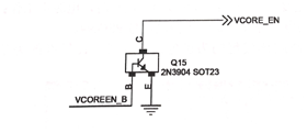
1.Turn on (EN) signal.
Turn on signal is the signal that controls chip to work, abbreviation EN, is abbreviation of ENABLE. Common open signals are high-level on-circuit operation, low-power normally closed circuit (see figure 1). There are also chip-on-off signals called SHDN#, the SHUTDOWN, band # number that indicates low level efficiency, which means that low power is normally turned off, so if you want to turn it on, it must be high.

Fig.1 EN signal circuit
The common names of EN signals are EN, ENLL, DVD, VR_Enable, OUTEN, ENABLE, SHDN#, VCORE_EN, VRM_EN, VTT_PWRGD, VRD_EN, etc.
2.Power Good (PG) signal.
POWERGOOD, is abbreviated to PG. The good signal of power supply is used to describe the signal of normal power supply, usually when the power level is high, the power supply is normal. For example, the ATX power supply uses gray lines as a good signal for (ATXPWROK) signals, and gray lines are designed to delay hundreds of milliseconds after electrification to indicate that the power supply is normal at a high level. For example, CPU power supply management chip in the normal issue of CPU voltage, will send a good signal to the South Bridge power supply VRMPWRGD chip, indicating that the power management chip work well.
The high level ATXPWROK signal from the ATX power gray line and the VRMPWRGD signal from the power supply chip in the main board will be sent to the Nanqiao chip to indicate that the corresponding power supply is normal, and the Nanqiao chip will issue CPUPWRGD to CPU, after receiving the good power supply signal. A reset signal is then generated to reset the entire motherboard and each device.
The common names for PG signals are PG,PWRGD, PWROK, ATXPWRGD,VTPWRGD,CPUPWRGD, VR_RDY, YRM_PWROK, and so on, as shown in figure 3.

Fig.2 Powergood
3.Clock (CLK) signal.
Clock signal CLK (CLOCK) is the digital circuit working reference, so that each connected equipment to work at a uniform pace. The basic unit of the clock signal is Hz. There is a master clock generation circuit on the motherboard that provides clock signals to all devices on the motherboard. For different devices, the clock circuit sends out different clock signals, such as the frequency of the clock signal given to CPU is above 100MHz. The clock signal frequency for the PCI device is 33 MHz, the clock signal frequency for the PCILE device is 100 MHz, and the clock signal frequency for the USB controller (integrated in the South Bridge chip) is 48MHz. The clock signals of CPU, PCI, PCL-E and so on need the normal power on the motherboard, and the clock chip can be measured by oscilloscope.
The motherboard requires that two connected devices must have the same frequency of clock signals and voltages to communicate, such as memory and North Bridge chips, both of which require the same clock signals and voltages in order to transmit signals normally.
4.Reset (RST) signal.
Reset RST (RESET (abbreviated) is the meaning of a fresh start. Now the device reset signal on the motherboard is from high level to low level jump back to high level. For example, the reset signal of PCI is from 3.3V to 0V and back to 3.3V, which is a normal reset jump process. The reset signal is generally expressed as *** RST#, such as PCIRST#,CPURST#,IDERST#, etc. Reset signal can only be instantaneous low level, the reset signal is high when the motherboard is working normally.
When you say no reset, you usually mean no reset voltage, that is, the reset signal measurement point voltage is 0V.


No comments:
Post a Comment