It is very simple to understand the principle of a common-emitter amplifier circuit. But it is not easy to really design a common-emitter amplifier circuit. Here is a summary of the design steps of the common-emitter amplifier.
1. Design requirements:
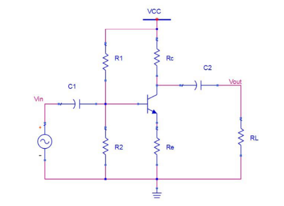
The following figure shows a RC-coupled common-emitter amplifier circuit. For a 1 kHz sinusoidal signal with an input peak-to-peak value of 2V, the load is 100kohm, and a 5x amplification circuit is designed.

2, design ideas and steps
The first step: First, the power supply voltage VCC must be selected.
In the circuit, the power supply voltage is high, and the power consumption is large. When possible, everyone should continuously reduce the power supply voltage to achieve low power consumption. In an amplifying circuit, the minimum supply voltage depends on the amplitude and amplification of the input signal. For example, to amplify the 2Vpp signal by a factor of 5, the limit VCC also needs to be greater than 10.5V (0.5V for V_ces and V_Re). The larger the supply voltage margin, the smaller the design pressure. Here, the common 15V voltage is taken as VCC.
Step 2: Design the value of Rc
The output impedance Rc of the common-emitter amplifying circuit needs to be set according to the magnitude of the load resistance. The value of the resistor in the circuit must be considered. If the bigger the better, it is better to open the circuit. If the smaller the better, the short circuit is better. The smaller the Rc is, the smaller the output impedance is, and the more stable the amplification factor is after the load is applied. However, the smaller the Rc, the larger the static power consumption of the amplifying circuit, that is, the power consumed without load.
Considering the load condition, set it to one tenth of the load 100kohm, so that 90% of the voltage will be added to the load, which has little effect on the amplification; Rc=10kohm.
The third step: design the value of Re
According to the magnification formula, A=-Rc/Re, the magnification is 5, so, Re=2kohm.
Step 4: Design the input signal bias voltage
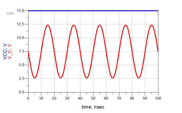
The common-emitter amplifier circuit is reverse-amplified, so the higher the DC offset of the input signal, the lower the output signal; the lower the input signal offset, the higher the output signal is. If there is no special requirement, the output signal can be placed in the center of the power rail (so that the maximum undistorted gain can be obtained), as shown in the figure below.

According to the DC equivalent circuit and Vc=7.5V, the DC offset Vb of the input signal can be deduced. Here we take the bias voltage Vb = 2.2V.
Step 5: Design the size of R1 and R2
Since the 15V partial voltage gets 2.2V, the higher the resistance power consumption, the lower the input impedance. However, since the voltage divider resistor network also has a branch flowing through the B pole of the triode, R2 must be small enough to ignore the current flowing through the branch. Calculated by beta=100, the equivalent resistance of the branch is 100*. Re=200kohm. Therefore, choose R2=20kohm, which is much smaller than the equivalent resistance of the branch.
According to R2 is 20kohm, R1=116kohm is calculated, 116kohm is not in the E24 series, and the closest R1 is 120kohm. This will bring a little DC error, but because the VCC margin is relatively large, some errors have no effect.
Step 6: Selection of electrolytic capacitors C1 and C2
The electrolytic capacitor must have an impedance to the AC signal close to zero. In other words, the use of electrolytic capacitors is related to the signal frequency. From the filter point of view, the capacitors C1 and R1 || R2 || beta * Re constitute a high-pass filter, as long as the high-pass filter cutoff frequency is lower than 1/10 of the signal frequency, the impedance of the input signal is considered to be 0, here Take C1=120nf. Similarly, the capacitor C2 and the load RL constitute a high-pass filter. As long as the cut-off frequency of the high-pass filter is lower than 1/10 of the signal frequency, the impedance of the output signal can be considered to be 0, where C2=20nf is taken.
If you want to know more, our website has product specifications for the common-emitter amplifier, you can go to ALLICDATA ELECTRONICS LIMITED to get more information


No comments:
Post a Comment