Friday, September 27, 2019

Hitachi integrates AI into the camera to enhance night pedestrian detection

Hitachi Automotive Systems said it has applied artificial intelligence (AI) technology to stereo cameras, which are designed for automotive automatic braking. The camera uses hundreds of thousands of data as "teacher data" to achieve night pedestrian detection. At present, various competitors are developing sensors that support AI. Hitachi Automotive Systems will supply this new sensor to Suzuki Motor Co., Ltd. in order to lead the commercialization of AI sensors.

According to the company, the new sensor's performance is much better than its competitors' products, able to detect pedestrians at night, and then the car can automatically brake, more braking performance than vehicles equipped with Israel Mobileye's main image processing chip EyeQ3 it is good.

Previously, Hitachi’s cameras were “rule-based” to identify objects, ie developers needed to set conditions manually, as did other companies’ products. However, the "rule-based" approach complicates conditions and makes it difficult to support nighttime object detection. This time, Hitachi uses machine learning technology to effectively find conditions in large amounts of data.

In general, a stereo camera uses two left and right cameras to take two images, and then uses the parallax between the two images to detect the shape of the object and the object located in front of the vehicle, and then use pattern recognition to determine the detected object. Whether it is a pedestrian. The stereo camera of Hitachi Automotive Systems will use machine learning to perform image recognition.

Hundreds of thousands of "teacher data" are stored in the image processing microcomputer of the new camera, and then the image taken by the camera is compared with "teacher data" to determine whether the object is a pedestrian. Previously, the stereo camera of Hitachi Automotive Systems used the normal pattern recognition method, which uses multiple images for judgment.

Even if the pedestrian is only illuminated by the headlights of the car or the entire body of the pedestrian can be seen, and the brightness of each body part is different, the camera uses machine learning, which is easier to detect than the traditional pattern recognition method.

The Hitachi Automotive System also increases the dynamic detection range of the CMOS sensor, reducing the F value of the lens (the smaller the F value, the larger the aperture) and doubling the sensitivity of the camera. Thanks to its dynamic range of motion detection, the camera captures both bright and dark objects. And because the F value is smaller, the camera is more likely to find pedestrians in the dark.

When machine learning techniques are applied to image recognition processing, the amount of data that needs to be processed is increased. In order to solve this problem, the Hitachi Automotive System has modified the microcomputer of the stereo camera to improve its performance. The previous stereo camera used three microcomputers for image processing, image recognition, and vehicle control. The new stereo camera of Hitachi Automotive Systems integrates only two microcomputers for image processing and image recognition. Then, the microcomputer for image recognition is upgraded from a single core to a dual core. As the number of cores increases, the microcomputer can not only use machine learning technology, but also improve the processing speed of image recognition.

How to use the position map on the microstar (MSI) motherboard.

1. Point Bitmap program installation.
Micro-star motherboard point bitmap view software is a ICGE program. IGE is a direct-running program that is used in the same directory as the IGE.DLL file, as shown in figure 1.
image.png
Fig.1 IGE programs and fil
Double-click directly to run the program, the program after the interface is shown in figure 2.

image.png
Fig.2 IGE Program button description


2. Tool description.
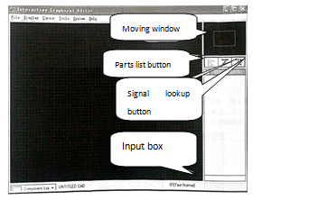
On the right side of the window is a selection and lookup toolbar with the corresponding tool buttons, as shown in figure 2.
(1) Window: click in different locations in the window and you can display components from different locations on the motherboard in the window.
(2) List of parts button: click to find the appropriate components.
(3) Signal lookup button: click to find the corresponding signal.
(4) Input box: input information when looking up components or signals.

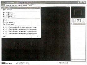
3.Sept1, click the File main menu, as shown in figure 3.
image.png
Fig.3 File Main menu
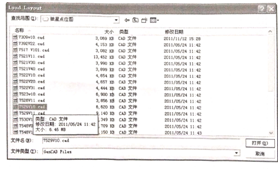
Step 2, click Doad Layout to find the point bitmap sequence source location, as shown in figure 4.
               image.png
Fig.4 Select Program source

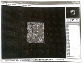
Step 3, select the program source and click the Open button to load the program source, as shown in figure 5.
image.png
Fig.5 Program source loading effect diagram


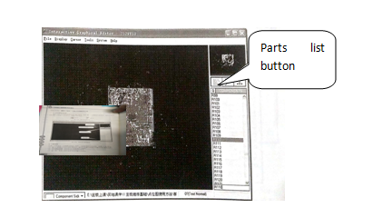
Step 4, click the parts list button and enter the find component location number R110 in the find box, as shown in figure 6.

 image.png
Fig.6 Component lookup input effect

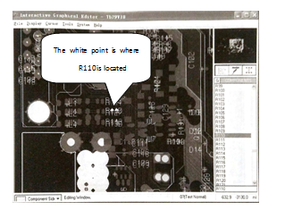
Step 5, double-click the R110 component tag, and then the mouse will direct to the R110 position, and the resistor R110 will display white, as shown in figure 7.
image.png

Fig.7 Component display effect diagram

4.Signal lookup method.
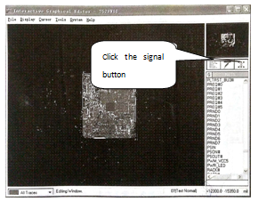
Step 1, click the signal Lookup button, as shown in figure 8.
 image.png
Fig.8 Signal lookup button

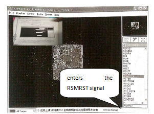
Step 2, enter the name of the signal you want to find in the input box, and this example enters the RSMRST signal, as shown in figure 9.
image.png

Fig.9 Signal input box

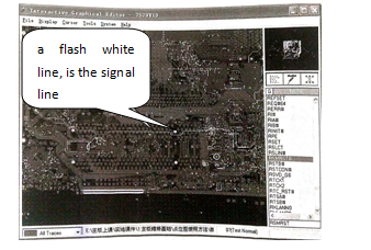
Step 3, double-click the corresponding name of the signal, in the window will be a flash white line, is the signal line, as shown in figure 10.
             image.png

Fig.10 Signal alignment effect diagram

5.Connection point finding method
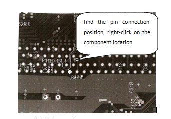
If you want to find the pin connection position, right-click on the component location, and then the connected line becomes white and flashes, as shown in figure 11, and the right-click again disappears.
image.png

Fig.11 Line route


This article is from Allicdata Electronics Limited. Reprinted need to indicate the source.

Saturday, September 21, 2019

What is the letter signal on the motherboard?

1.Turn on (EN) signal.
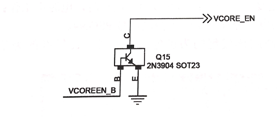
Turn on signal is the signal that controls chip to work, abbreviation EN, is abbreviation of ENABLE. Common open signals are high-level on-circuit operation, low-power normally closed circuit (see figure 1). There are also chip-on-off signals called SHDN#, the SHUTDOWN, band # number that indicates low level efficiency, which means that low power is normally turned off, so if you want to turn it on, it must be high.
               image.png
                      Fig.1 EN signal circuit

 The common names of EN signals are EN, ENLL, DVD, VR_Enable, OUTEN, ENABLE, SHDN#, VCORE_EN, VRM_EN, VTT_PWRGD, VRD_EN, etc.
               
2.Power Good (PG) signal.
POWERGOOD, is abbreviated to PG. The good signal of power supply is used to describe the signal of normal power supply, usually when the power level is high, the power supply is normal. For example, the ATX power supply uses gray lines as a good signal for (ATXPWROK) signals, and gray lines are designed to delay hundreds of milliseconds after electrification to indicate that the power supply is normal at a high level. For example, CPU power supply management chip in the normal issue of CPU voltage, will send a good signal to the South Bridge power supply VRMPWRGD chip, indicating that the power management chip work well.
The high level ATXPWROK signal from the ATX power gray line and the VRMPWRGD signal from the power supply chip in the main board will be sent to the Nanqiao chip to indicate that the corresponding power supply is normal, and the Nanqiao chip will issue CPUPWRGD to CPU, after receiving the good power supply signal. A reset signal is then generated to reset the entire motherboard and each device.
The common names for PG signals are PG,PWRGD, PWROK, ATXPWRGD,VTPWRGD,CPUPWRGD, VR_RDY, YRM_PWROK, and so on, as shown in figure 3.
         image.png
                     Fig.2 Powergood
          

3.Clock (CLK) signal.
Clock signal CLK (CLOCK) is the digital circuit working reference, so that each connected equipment to work at a uniform pace. The basic unit of the clock signal is Hz. There is a master clock generation circuit on the motherboard that provides clock signals to all devices on the motherboard. For different devices, the clock circuit sends out different clock signals, such as the frequency of the clock signal given to CPU is above 100MHz. The clock signal frequency for the PCI device is 33 MHz, the clock signal frequency for the PCILE device is 100 MHz, and the clock signal frequency for the USB controller (integrated in the South Bridge chip) is 48MHz. The clock signals of CPU, PCI, PCL-E and so on need the normal power on the motherboard, and the clock chip can be measured by oscilloscope.
The motherboard requires that two connected devices must have the same frequency of clock signals and voltages to communicate, such as memory and North Bridge chips, both of which require the same clock signals and voltages in order to transmit signals normally.

4.Reset (RST) signal.
Reset RST (RESET (abbreviated) is the meaning of a fresh start. Now the device reset signal on the motherboard is from high level to low level jump back to high level. For example, the reset signal of PCI is from 3.3V to 0V and back to 3.3V, which is a normal reset jump process. The reset signal is generally expressed as *** RST#, such as PCIRST#,CPURST#,IDERST#, etc. Reset signal can only be instantaneous low level, the reset signal is high when the motherboard is working normally.
When you say no reset, you usually mean no reset voltage, that is, the reset signal measurement point voltage is 0V.

Thursday, September 19, 2019

How to measure insulated gate bipolar transistors?

( 1 ) Measure the three foot of IGBT with multimeter RX10kΩ without damping tube, one of which is infinite with the other two feet, this foot is G, and the other two feet are C and E.
In the test, there are two feet with a certain resistance, a small resistance, such as NPN type pipe, the black pen is connected to E, the red pen is connected to C; the PNP type is the opposite.

( 2 ) Measuring three electrodes with RX 10Ω ~ RX 100Ω for measuring the damping pipe. The secondary resistance is several hundred ohms, and the other one is several thousand ohms. The two feet are C and E, and the resistance is small, and the black pen is the E-pole,red stylus is the C pole, the other foot is the B pole ( G pole ).

( 3 ) When measuring and measuring IGBT module , the resistance between CE, CB and BE of IGBT should be measured by using the RX 10Ω of the multimeter, which should be in accordance with the resistance of the damping pipe. If the IGBT component fails , there may be a short circuit between the collector and emitter, collector and gate. ( note : when IGBT works, the voltage between the gate and emitter is about 9V, and the emitter is the reference. If you use the road measurement method, you should first disconnect the corresponding pin, to prevent the circuit due to the impact of internal resistance caused by false judgment.

If you want to know more, our website has product specifications for the IGBTs, you can go to Allicdata Electronics Limited to get more information.

IGBT :  HGTD1N120BNS9A
HGTD1N120BNS9A Allicdata Electronics

IGBT module :  IXGN320N60A3

IXGN320N60A3 Allicdata Electronics

Wednesday, September 18, 2019

What is the main application of MEMS sensors?

1, medical
MEMS sensor is applied to non-invasive fetal heart rate detection. It is a very technical job to detect fetal heart rate. Because the fetal heart rate is very fast, between 20 and 160 times per minute, with traditional stethoscope or even ultrasound Doppler with amplification. It is difficult to measure accurately with manual counting. Ultrasound Doppler fetal heart rate monitors with digital display are expensive and are used only in a few large hospitals. In addition, the ultrasonic vibration wave acts on the fetus, which has a great adverse effect on the fetus. Although the detection dose is very low, it is also a lossy detection category and is not suitable for regular, repetitive inspections and home use.

Based on VTI's MEMS accelerometer, a non-invasive fetal heart rate detection method was developed to develop a simple, easy-to-learn, intuitive and accurate clinical diagnosis between the fetal heart stethoscope and the Doppler fetal monitor auxiliary instrument. The fetal heart rate is converted into an analog voltage signal by an acceleration sensor, and the difference is amplified by an instrument amplifier for preamplification. Then, a series of intermediate signal processing such as filtering is performed, and the analog voltage signal is converted into a digital signal by an A/D converter. The optical isolation device is input to the single chip microcomputer for analysis and processing, and finally the processing result is output.
The fetal heart rate monitor based on the MEMS accelerometer design can be used as a terminal to make a remote fetal heart rate monitoring system. The central signal collection and analysis monitoring host at the hospital side gives the automatic analysis result, and the doctor diagnoses the result. If there is any problem, the pregnant woman is notified to the hospital in time. This technology is beneficial for pregnant women to check the condition of the fetus at any time, which is conducive to the health of the fetus and pregnant women.

2, car
MEMS pressure sensors are mainly used to measure airbag pressure, fuel pressure, engine oil pressure, intake line pressure and tire pressure. The sensor uses single crystal silicon as a material to form a force sensitive diaphragm in the middle of the material by MEMS technology, and then diffuses impurities on the diaphragm to form four strain resistors, and then connects the strain resistors into a Wheatstone bridge. Circuitry to achieve high sensitivity. Automotive MEMS pressure sensors are available in several common forms such as capacitive, piezoresistive, differential transformer, and surface acoustic wave.

The principle of MEMS accelerometer is based on Newton's classical mechanics law. It is usually composed of suspension system and detection quality. The acceleration is detected by the offset of micro silicon mass. It is mainly used in automotive airbag systems, anti-skid systems, and car navigation. In addition to capacitive and piezoresistive systems, MEMS accelerometers include piezoelectric, tunneling current, resonant, and thermocouple types. Among them, the capacitive MEMS accelerometer has the characteristics of high sensitivity and minimal temperature influence, and is the mainstream product in MEMS micro accelerometer.
The microgyroscope is an angular rate sensor, which is mainly used for GPS signal compensation and automobile chassis control systems for car navigation, mainly including vibrating type and rotor type. The most widely used is a vibratory gyroscope that senses the angular velocity by using the Coriolis effect generated by the vibration mass of single crystal silicon or polycrystalline silicon when it is rotated by the susceptor. For example, when the car is turning, the system measures the angular velocity through the gyroscope to indicate whether the rotation of the steering wheel is in place, and actively applies appropriate braking on the inner or outer wheels to prevent the car from getting out of the lane. Usually, it forms active control together with the low accelerometer system.

3, motion tracking
In the daily training of athletes, MEMS sensors can be used to measure 3D human motion, record each action, and the coaches analyze the results and compare them repeatedly to improve the athletes' performance. With the further development of MEMS technology, the price of MEMS sensors will also decrease, which can be widely used in the Volkswagen gym..
In terms of skiing, pressure sensors, accelerometers, gyroscopes and GPS in 3D motion tracking allow users to obtain extremely accurate viewing capabilities. In addition to providing snowboard movement data, they can also record the user's position and distance. The same is true for surfing. The 3D motion tracking installed on the surfboard records information such as sea level, speed, surfing time, paddle distance, water temperature and calories burned.

4, mobile phone photo
Before the advent of MEMS Drive, the mobile phone camera was mainly operated by the voice coil motor to move the lens group to achieve anti-shake (referred to as the lens anti-shake technology), which was greatly limited. Another high-end anti-shake technology in the market: multi-axis anti-shake, the use of mobile image sensor  to compensate for jitter, but because of the huge size of this technology, power consumption exceeds the mobile phone load, has been unable to on the phone application.

Tuesday, September 17, 2019

How to detect whether the trigger circuit related signal is normal?

After the standby condition detection is normal, the trigger signal in the trigger circuit is detected whether the jump-off is normal or not. The common trigger signals are PWRBITN#, SLP_S3#, PSON#. Trigger circuit maintenance methods are as follows.

 (1) First distinguish the main board trigger circuit working mode, common main board trigger circuit work as follows.
Intel, nVIDIA, AMD chipset motherboard: Switch, IO chip, south bridge chip, IO chip green wire.
VIA chipset motherboard: Switch south bridge chip transistor green wire. 
SIS chipset motherboard: Switch South Bridge chip green cable. 
Intel original motherboard: Switch South Bridge chip IO chip, detect CPU green cable.
IBM, DELL motherboard: Switch South Bridge chip IO chip green cable. 

(2) Measuring the corresponding trigger signal. 

a) Most of the motherboards are triggered by IO chips in the existing motherboard maintenance, so to measure the trigger signal you must measure the IO chip-related pins. Common IO chips trigger pin as follows. 
Pin of IT8702, IT8712, IT8716, 1T8718, 1T8720, IT8721, 1T8726, 178728: 67 powered, 75 72 71 76 (GB plus 31). 

IT8758 pin: 2, 31 power, 35 33  32 36. 
Pin position of W83627: 61 Power, 68 67 73 72. 
Pin position of F71872: 67 power, 75 72  71 76. 
Pin position of F71862, 71882, 71883: 68 electricity, 80 81 82 83. 
Pin position of F71889: 65 power supply, 76 77 78 79. 
Note: IT8705, W83697, W83687 are not triggered. 

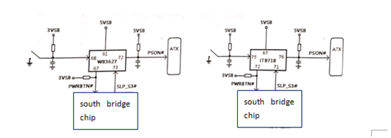
b) The trigger circuit block diagram commonly composed of Huabang and Lianyang I 0 chips is shown in figure 3. 

image.png
(a) Huabang                      (h) Lianyang
figure 3 IO chip trigger block diagram.

Huabang and Lianyang 1O chip corresponding to normal foot jump mode: trigger switch before triggering switch triggering switch after. 
W83627 Series. 
The 68 pin are high level low level high level. 
The 67 pin are high level low level high level. 
The 73-pin is low or high-level continuous high-level. 
The 72-pin is high-level sustained low-level. 
ITE series (except IT8711). 
The 75-pin is high-level low-level high-level. 
The 72-pin is high-level low-level high-level. 
The 71-pin is low or high-level continuous high-level. 
The 76-pin is high-level sustained low-level.

(3) Abnormal maintenance method of trigger signal. 
Using W83627 series IO chip motherboard, trigger circuit maintenance ideas are as follows. a. if the switch does not have a high level, check the pull-up resistance, capacitance, and IO chip of the switch for damage.
b. if the switch has a high level, but presses the switch 68 pin without jumping, check the line (run) from the switch to 68 pin.
c. if the 67 pin in front of the switch do not have 3.3V, check first whether the power supply to the IO chip is normal or not. If normal first change the IO chip, and finally change the South Bridge chip.

Wednesday, September 11, 2019

Special resistance: How to use network resistors and adjustable resistors?

l  Network resistors
In the circuit design, the network resistor is also used. The network resistor has the advantage of being neat and less space-consuming than the color ring resistor. The inside of the circuit is actually arranged neatly by a plurality of resistors. There are two types of network resistors.
Note: Network resistors are the resistors commonly used in circuits.

1.Dual in-line network resistor
The dual in-line network resistor is similar to the IC. The first pin is represented by a dot or a small groove. When you hold the component, the component body faces itself, the slot or small dot is up, and the first one on the left. The pin is the first pin. The holes for the first pin are usually marked on the board with square or pointed pads. When plugging in the network resistor, the first pin must be inserted into the board with the hole labeled the first pin.

2.Single in-line network resistor
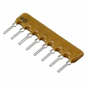
A single in-line network resistor is a plastic box with a row of pins. The symbol in the circuit is "RN
RP", "1B"
The first pin is indicated by a small dot on the component body or the number "1" or a thick solid line. The first pin on the board is usually represented by a square pad or a dot. The first pin is usually inserted into this square pad or next to a small dot.

Network resistor :4608X-101-181LF
 4608X-101-181LF.png


l  Potentiometer : adjustable resistor
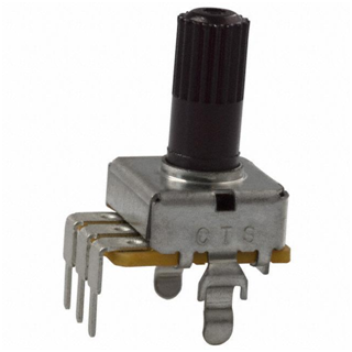
The potentiometer is an adjustable resistor. Its  symbol in circuit is Rp. The resistance can be changed by adjusting the knob or screw on the component body. The potentiometer is directional. A potentiometer has three pins and there is only one way to insert the potentiometer into the board. The shape of the potentiometer is square, circular and rectangular.
Generally speaking, it is easy to judge the quality of the resistor by using a multimeter:
In general, it is easy to judge the quality of a resistor using a multimeter:
Adjust the resistance block of the multimeter to the appropriate resistance value and placing the two test leads on both ends of the resistor.
It should be noted that the hand cannot touch the metal part of the test lead when testing the resistance. In actual electrical maintenance, resistance damage rarely occurs. The important thing to note is whether the resistor is soldered (false solder) or stripped. The shape of the resistor is shown in the figure.

Potentiometer : 296UD103B1N


image.png

Tuesday, September 10, 2019

Debug Stellar Automotive Microcontroller

By STMicroelectronics PLS programmable logic simplifies software development and systems support, Stellar automotive microcontroller architecture for this powerful debugging, tracking and testing.

As the combination of several new technologies on the chip, the chassis and the telephone-assist auxiliary system (ADAS) can be implemented with a power system that is controlled by a personalized microcontroller series "Star". With the six Arm Cortex R52, the first building block generated by the latest microcontrollers is also the core clock frequency of 400 MHz. Together with 16 MB of embedded phase change memory (PCM), it provides high multicore performance for real-time applications.

Further, Stellar series also has a variety of security and protection features, including a hardware security module (HSM) function and a lock-step. Management software program for the separation and storage protection enhances the security and reliability features.

The Stellar range meets the stringent requirements of the automotive electronics system ISO 26262 to ASIL-D safety standards. In addition, three floating-point Cortex-M4 cores and DSP extensions act as application-specific accelerators. Due to the long-term close cooperation with STMicroelectronics, PLS has been able to develop optimized debugging and tracking tools for the ST-Partner Program to develop members with the first home from the Stellar to be able to provide this complex automotive microcontroller architecture.

With multi-core run control, UDE's specific features, you can use the built-in debug logic to synchronize start and stop of all cores or selected groups. Multi-core breakpoints that can be used in shared code simplify the debugging of complex applications. Such a breakpoint is always valid no matter which kernel is currently executing the code. In addition to support for the actual application kernel, UDE also allows debugging of hardware security modules integrated on the Stellar MCU. To this end, HSM can be integrated into multi-core operational control.

The optimized programming of phase change memory (PCM) implemented in the Stellar family of modules is achieved by means of the UDE Memtool flash programming tool integrated in UDE. Phase change memory allows for faster, safer, and more accurate programming than traditional flash programming. In practice, this means, for example, that even a single byte can be written, whereas only the entire block could have been written before. Due to the nature of the PCM, the over-the-air software (SOTA) for this storage technology can be used particularly efficiently and reliably. The special features of UDE Memtool ensure the smooth support of SOTA.

For detailed analysis of multi-core applications at the system level, the UDE supports a wide range of trace capabilities for the CoreSight debug and trace scheme, where the arm is in the Cortex-R52-core core of the Cortex-M4, and for the connection to the chip has been achieve.

The family of three devices UAD2pro, UAD2next and UAD3 + PLS universal access devices are also reliably debugged to the stellar microcontroller family via JTAG or arm-specific serial line debug (SWD) interfaces. It is ideal for capturing and storing large amounts of trace data while UAD3+, which is available on the Star MCU with up to 4 GB of trace memory in the special tracking POD for High Speed Serial Trace Port (HSSTP),

Monday, September 9, 2019

How does the Intel H55 chipset motherboard reset circuit work?

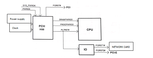
The reset circuit for the Intel single-bridge H55 chipset motherboard is shown in figure 1.
image.png

Figure 1 Intel single bridge H55 chipset motherboard reset circuit.
1. Short switch, the main board circuit began to work, through the supply circuit step-down to generate internal power supply, bridge power supply, bus power supply and CPU power supply voltage.

2. After the CPU power supply is stabilized, the power management chip outputs a high-level VR_RDY signal. The conversion of the circuit to the SYS_ PWROK bridge indicates that the CPU power supply is normal.

3. After the output voltage of ATX is stable, the ATX _ PWROK signal is delayed outputted to the 1O chip, and the high-level PWROK signal is output to the bridge through the internal conversion of the 1O chip, indicating that the power supply of the ATX power supply is normal.

4. After the mainboard power supply is normal, turn on the clock circuit to work, output the clock signal to the bridge.

5. The bridge power supply, the clock signal is normal, after receiving two PG signals, sends out the high level DRAMPWRGD signal to the CPU, to indicate the memory power is normal.

6. The bridge re-outputs the PROCPWRGD signal to the CPU, to indicate full board power supply is normal.

7. The bridge sends out a reset signal for the PLTRST# platform to reset the IO chip and the CPU.

8. The bridge finally issues the PCIRST# reset PCI slot.

9. After receiving the reset signal from the bridge, the IO chip generates the PCIRST2# reset PCI_E slot through the internal logic circuit, and the PCIRST1# reset the Nic chip.
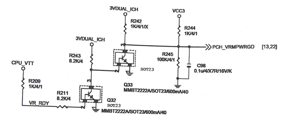
The SYS_ PWROK signal generation circuit is shown in fig. 2. After the power management chip is stabilized, the output high-level VR RdY signal is pulled up through R209 and sent to the B pole of Q32 through R221, making Q32 on and Q33 cut-off. The PCH VRMPWRGD is pulled to 3.267V high through the R244 and R245 partial voltages, and the SYS_PWROK pin sent to the bridge indicates that the CPU is powered properly.
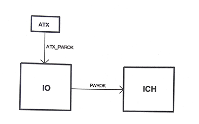
The principle of PWROK signal generation is shown in figure 3. ATX power output high-level ATX PWROK signal to the IO chip, after the internal logic conversion of the IO chip, output PWROK high-level 3.3V signal to the South Bridge chip to indicate that the power supply is normal. The common Huabang W83627 series IO chip outputs the PWROK signal from 71 pins to the South Bridge chip, and the Lianyang Series IO chip outputs the PWROK signal from 32 feet or 78 feet to the South Bridge chip.
image.png
Fig.2 SYS_PWROK signal generation circuit.
image.png
Fig.3 PWROK signal generation circuit.

Saturday, September 7, 2019

Measure whether the startup circuit board is shorted.

Measure if the motherboard is significantly short-circuited. There are 3VSB standby power supply, USB interface data cable, CPU power supply, memory power supply, bridge power supply, bus power supply and so on.

The measurement short circuit causes the Multimeter to contact the position of the diode, the red pen contact ground, the black meter pen contact position, and the display screen shows the value of the bipolar value between the measured point and the ground.

1.If the 3VSB is short-circuited to the ground. The measured position is the A14 foot of the PCI slot or the B10 foot of the bounded PCI-E slot.
(1)If you confirm the 3VSB short circuit to the ground, remove the Nic chip in turn. 1394, part of the motherboard  IO chip, fixed output 3.3V 1117, South Bridge chip.

(2)If the short circuit is uncertain, can touch the Nic chip in standby state, IO chip, Nanqiao chip and so on are hot, and the standby voltage is low, etc., to judge whether the 3VSB is short circuit or not.

2. If the cable is short-circuiting to the ground. The normal value of the polar to the earth is about 400 ~600.

(1)Measure the USB data line, if any of the data lines short-circuit to the ground, determine that the South Bridge chip is bad.

(2)To measure the USB data line, if any of the data lines to infinite value, first check whether the USB interface to the South Bridge chip between the broken wire, no broken wire is the South Bridge chip empty welding or South Bridge chip broken.

3. If VCORE is short-circuiting to the ground. Generally, the dipolar value of the earth is higher than 30, but the accurate judgment needs to be compared. If short circuit, first check whether FET uses LD1010D, LD1014D, if not, then remove tantalum capacitor, power chip, lower tube, drive chip, filter capacitance, 478 main board of the South-North Bridge chip and so on.

4. Whether the memory, AGP video card, bridge, bus power supply, etc., is short-circuit to the ground. The chip group is similar to the same value, not 0 can not determine short circuit, using a comparative method to judge (test spots: coil measuring coil pin, no coil measuring field effect tube S pole). If a short circuit is determined, it is usually a bridge short circuit, rarely a field effect transistor and capacitor failure.
This article is from Allicdata Electronics Limited

Friday, September 6, 2019

Introducing a single-chip/mixed digital-to-analog converter

This article briefly introduces Monolithic/Hybrid Digital to Analog Converters
DIGITAL TO ANALOG CONVERTERS,both of them have been designed for four inputs. But, if the number of inputs is more than four, the combination of output becomes more than 16. This makes the circuit more complex and the accuracy of the circuit reduces. Therefore, in critical and complex applications, a monolithic/hybrid D/A converter IC must be used. With the help of binary-weighted resistor, and R  and 2R resistor methods, 8-bit,10-bit, 12-bit, 14-bit, and 16-bit D/A converters can be designed with a current output, voltage output, or both current and voltage outputs.
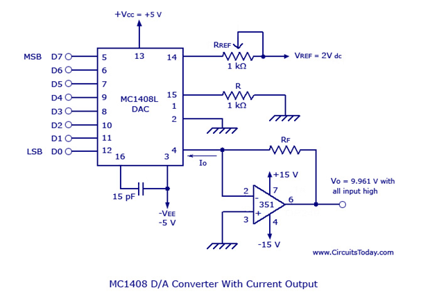
The most commonly used 8-bit D/A converter is MC 1408 which has a current output that can be converted to a voltage type using a current to voltage converter op-amp. The design along with the current to voltage converter is shown in the figure below.
image.png
MC 1408 Digital to Analog Converter
V0 = Vref/Rref *(RF)*{D7/2 + D6/4 + D5/8 + D4/16 + D3/32 + D2/64 + D1/128 + D0/256}
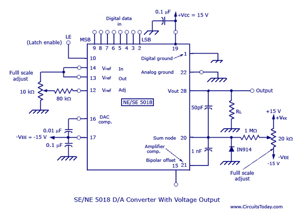
SE/NE 5018 is a typical 8-bit D/A converter with voltage output. The figure is shown below.
image.png
SE-NE 5018 Digital to Analog Converter
In the figure, the SE/NE 5018 circuit is configured for uni-polar output (0V to 10V). For 12 bits of resolution as well as current and voltage outputs, hybrid D/A converters such as DATEL DAC-H2 series is used.
For the correct selection of the D/A converter out of the lot, some important specifications of the converter must be known.
This article is from Allicdata Electronics Limited. Reprinted need to indicate the source.

What issues need to be considered when designing LED driver circuits?

LED has many advantages such as environmental protection, long life, high photoelectric efficiency, etc. In recent years, the application in...