Friday, June 28, 2019

What is the step-down working principle of capacitor?

Capacitor buck LED driver circuit is often used in the drive circuit of small current LED due to its small size, low cost and relatively constant current.

The capacitor buck LED driver circuit uses the capacitive reactance generated by the capacitor at a certain AC number to limit the maximum operating current. For example, at a operating frequency of 50 Hz, a 1 μF capacitor produces a capacitive reactance of approximately 3180 Ω. If an AC voltage of 220 V is applied across the capacitor, the maximum current flowing through the capacitor is approximately 70 mA. But no power is generated on the capacitor, because if the capacitor is an ideal capacitor, the current flowing through the capacitor is the imaginary current, and the work it does is reactive power (the capacitor belongs to the energy storage component).

According to this feature, if a resistive element is connected in series on a 1 μF capacitor, the voltage obtained across the resistive element and the power dissipation it generates are completely dependent on the characteristics of the resistive element.
For example, a 110V/8W bulb is connected in series with a 1uF capacitor and connected to an AC voltage of 220V/50Hz. The bulb is illuminated and emits normal brightness without being burned. Because the 110V/8W bulb requires 8W/110V=72mA. It is consistent with the current limiting characteristics of the 1uF capacitor.
Similarly, a 65V/5W bulb and a 1uF capacitor can be connected in series to a 220V/50Hz AC, and the bulb will be illuminated without being burned. Because the operating current of the 65V/5W bulb is also about 70mA. Therefore, the capacitor buck is actually using the capacitive reactance current limit, and the capacitor acts as a limiting current and dynamically distributing the voltage across the capacitor and the load.

The conventional method of converting AC power to low-voltage DC is to use a transformer to step down and then rectify and filter. If it is limited by factors such as volume and cost, the simplest and most practical method is to use a capacitor buck power supply.

When designing the circuit, the exact value of the load current should be measured first, and then the capacity of the step-down capacitor should be selected. Capacitor buck application circuit diagram, as shown in figure below
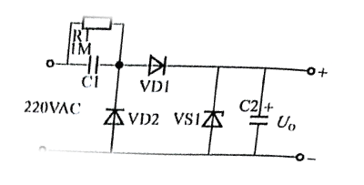
image.png
Since the current Io supplied to the load through the step-down capacitor C1 is actually the larger the charge/discharge current Ic C1 flowing through C1, the smaller the capacitive reactance Xc is, the larger the charge and discharge current flowing through C1 is. When the load current Io is less than the charge and discharge current of C1, excess current flows through the Zener. If the maximum allowable current Idmax of the Zener diode is less than Ic-Io, it will easily cause the Zener diode to burn out. In order to ensure reliable operation of C1, the withstand voltage selection should be greater than twice the supply voltage. The bleeder resistor R1 must be selected to vent the charge on C1 for the required time.

This article is from Allicdata Electronics Limited
Wednesday, June 26, 2019

New amplifiers with audio applications - IC and multi-chip modules

Infineon is combining its existing line of amplifiers with audio applications - IC and multi-chip modules. Four new Merus brand IC amplifiers have been proposed.

With its new "Merus" brand for audio amplifier ICs, Infineon wants to highlight the advantages of its amplifier ICs:
1. When the sound is generated in the speaker, the heat is not distributed;
2. Can't see, but can hear it;
3. Small and light;
4. Be flexible and configurable, but not just delicate and difficult to use.

The Merus amplifier is based on a new technology: multi-stage switching technology for Class D audio amplifiers, comparable to multi-level converter technology. Not only does it provide high efficiency, but it also has a positive impact on other audio amplifiers such as sound quality, size, output power, electromagnetic emissions and component costs.

Under the new Merus brand, Infineon bundles its amplifier ICs for audio applications.
Infineon is modulating the new Class D audio amplifier to control the power level of the analog five-speed converter. These multistage Class D amplifiers use additional power MOSFETs (integrated in the IC) and capacitors compared to conventional amplifiers.
This technique makes it possible to output an audio signal with a higher granularity, ie with a higher switching frequency and a scalable output signal level. Another advantage of multi-stage Class D amplifiers: they allow for smaller designs and sleep modes with virtually no measurable switching losses.

Four new Merus amplifiers
Based on the new modulation technology, Infineon introduces one of four integrated multi-stage class D audio amplifiers: the MA12040 and MA12070 with analog audio inputs, MA12040P and MA12070P with digital inputs (I 2 S). They are satisfied with power consumption in the 250 mW range and have no output filter. Therefore, they are particularly suitable for portable battery powered devices and for applications with limited installation space - if there is no space for the heat sink and the output filter is present.

The new Merus Class D amplifiers from the Infineon MA12040 / P and MA12070 / P support up to four channels.
Traditional Class D amplifiers operate only at higher volume levels and are more efficient. A realistic and typical audio playback that requires an average of about 1 watt of output power for itself is much more power than the IC of the first generation Merus multi-stage class d audio amplifier now presented.
The new audio amplifier IC supports up to four channels in the mode PBTL (parallel bridge load), BTL (bridged load) or SE (single-ended) can be configured. In PBTL mode, a single monolithic IC can deliver up to 160 W of peak power - maximum. 16 A load current. Alternatively, a four-channel IC can also be used in a 2.1 system, for example, two to drive a 20 watt range speaker (SE mode) and a 40 W woofer (BTL mode).
The new Merus Class D amplifiers, the MA12040/P and MA12070/P, have an integrated digital power supply with low distortion (THD + N = 0.003%) and low EMI emissions. They are protected by a variety of built-in functions: undervoltage shutdown (UVLO), short/overcurrent and DC protection, and warning and error messages when overheating. Infineon offers an integrated Merus Class D audio amplifier IC in a thermally optimized 64-pin QFN package with EPAD (exposed thermal pad).

Monday, June 24, 2019

The working principle of the start-up circuit of AMD dual-bridge RS880 chip board.

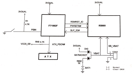
The AMD RS880 set motherboard power-up circuit works as shown in figure 1.
image.png 
Figure 1 operating principle block diagram of AMD RS880 chipset motherboard boot circuit.

Stage 1: after the CMOS battery is installed on the main board, the positive electrode of the battery passes through R692 and D43 to generate VBAT to power the RTC circuit inside the South Bridge chip. VBAT gets the high level SB _ VBAT signal from the JCMOS jumper cap to the South Bridge chip, and resets the RTC circuit inside the South Bridge Chip. The South Bridge chip supplies power to the crystal oscillator and the crystal oscillator starts to produce the 32.768kHz frequency to the South Bridge chip. The RTC circuit inside the South Bridge chip begins to work and is used to save the CMOS settings.

Stage2: the ATX power supply is turned on 220V alternating current, and the ATX power supply is output 5VSB power supply. After the step-down circuit is converted into 3VDUAL, the standby power supply is provided for the North Bridge chip and the IO chip. The IO chip sends out RSMRST_IO signal to the South Bridge chip after internal delay to indicate that the standby voltage is normal. So far, standby circuit work is complete.

Stage 3: the short switch generates the PSIN signal to the 10 chip, the 10 chip outputs the PWRBTN# signal of the 3.3V-0V-3.3V jump through the internal logic conversion and requests the power on the South Bridge chip. When the North Bridge chip receives the power-on request signal and its standby condition is normal, 3.3V continuous high-level SLP_S3# is output to the IO chip through the internal logic conversion, indicating that the power-up is allowed. Finally, the IO chip outputs the sustained low level ATX _ PSON# signal through the internal conversion, and pulls down the green line of the ATX power supply to complete the power-up.

This article is from Allicdata Electronics Limited. Reprinted need to indicate the source.

Saturday, June 22, 2019

Extend the life of electrical appliances

From the battery of the phone to the washing machine, the power converter is installed in a variety of ways. They are often the cause of failure of household appliances. A controller with a microprocessor can help to improve this problem.

The power converter converts the alternating current connected to the house into the direct current of the appliance. However, they are often prone to errors, which can adversely affect the life of the appliance. The Karlsruhe Institute of Technology (KIT) has now successfully developed a more durable power conversion that extends the life of appliances.

This power converter is based on a microprocessor. Installing electrolytic capacitors in a common power supply makes them light and compact, but it is also prone to failure. Although film capacitors are more durable, they require up to ten times more space, which increases component size.

At the Institute of Light Technology (LIT) at KIT there is now a digital control method developed that allows for the establishment of film capacitors that do not have significant variations in size.

Tip: The controller runs on the microprocessor and detects environmental effects such as voltage fluctuations and adjusts them. Therefore, a film capacitor having a lower capacitance value can be mounted, which reduces the element size. The use of less susceptible film capacitors extends the life of the appliance by a factor of about three, which reduces the company's maintenance effort. In addition, the new power unit offers the option of remote maintenance and integration into the Internet of Things.

What is the difference between a transformer and a coupled inductor?

Two inductors coupled together can be defined as separate components that share some of their flux lines. Due to the common coupling, one winding induces a voltage in the other winding: this is called mutual coupling.

Transformers, which are actually intended as "transfer" and signal impedance matching components, even nowadays certainly apply to the energy used in the sense of "conversion", ie the transfer of voltage and current.
image.png

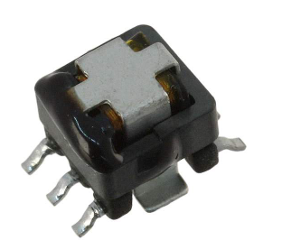
The two components - the coupled inductor and the transformer - are very similar on the surface. However, their parameters are optimized differently, and because of the difference between the named coupled inductor and the transformer, it is necessary to clarify the different uses.
Of course, in the end only the data table shows which parameters the component has and where they can be used. The transformer is specifically designed to transfer power from one winding to another. The coupling between the two windings must be as good as possible and the leakage inductance is close to zero. For this type of application, the absolute inductance of a single winding is usually secondary.

The transformer transfers energy directly from the primary winding to the secondary winding without storing energy in the magnetic circuit. For this purpose, current flows simultaneously in both windings, their magnetic fluxes being oppositely polarized and canceling each other out. Standard transformers are usually designed with fixed coupling to achieve values above 99%.

Typically transformers are used for power transmission where reduced coupling results in losses and inefficiencies. Coupled inductors have different strength couplings, from very low couplings, typically only 5% to 10% to over 90%.

In a transformer, an AC voltage is typically applied to the primary winding to generate a voltage on the secondary side, and power transfer occurs here immediately. Any portion of energy stored is often considered a problem because it can cause damage. Most transformers are wound on the core with low reluctance. Although the core has magnetization and leakage inductance, these are caused by parasitic effects.

An ideal transformer does not have these parasitic properties; an ideal transformer cannot store energy. The coupled inductor can store energy in accordance with an embodiment. The inductor is then designed to store considerable energy in the magnetic flux.

For this reason, the core has gaps, discrete gaps or distributed, such as iron powder cores, where the energy is stored as a magnetic field. Furthermore, the ferrite material and the winding structure are suitable for the corresponding type of coupled inductor.

For coupled inductors, each winding is still used alone as the actual inductor, although "some mutual coupling" of course acts as a circuit technology, there will be two separate inductors. Generally, stray inductance is not a problem for coupled inductors.

In fact, it may be useful to provide some guaranteed, low, uncoupled inductance or leakage inductance for each winding. The absolute inductance of each winding when the secondary winding is turned on is a precisely defined important parameter. Most of these coupled inductors have the same number of turns - a 1:1 gear ratio, but some special types have a higher gear ratio of 1:50 or higher.

The mutual coupling of a coupled inductor of the magnetic circuit at the magnetic flux produced by the windings is of the same polarity and is interesting such that, in addition, this results in a non-negligible value of the magnetic flux and magnetic energy is stored at the core.

Applications for coupled inductors typically include the use of separate inductor circuits, but one of the two coupling functions between the two inductor circuits facilitates the function of one or more circuit parameters. A coupled inductor can be used, for example, in a flyback converter where it stores energy while the switching transistor (MOSFET) is turned on and then transfers energy to the output when the switching transistor (MOSFET) is turned off.

Coupled inductors have many other advantages, such as significantly reduced current ripple, voltage conversion, changing circuit impedance, and galvanic isolation. For example, switching power supplies include SEPIC converters, galvanically isolated converters, multiphase converters, and special converter circuits that mitigate the negative characteristics of hard switching.

However, coupled inductors also have disadvantages, which result in inductors having, for example, slightly higher losses and non-ideal operations in the flyback converter, such as round, rather than causing triangular waveforms that must be considered in the circuit. In addition, the current specifications of the coupled inductor differ depending on whether their windings are connected in series or in parallel.

For example, when the windings are connected in series, the equivalent inductance due to mutual inductance is greater than twice the rated inductance. Unless otherwise specified in the data sheet, the saturation and RMS current ratings must be applied to both current flowing through the two windings. Therefore, a clear understanding of the operation and specifications of coupled inductors is critical to making the most of these devices.

LED strobe causes

When assessing the influence of light source on the human eye, it is inevitable to mention stroboscopic. With the advancement of electric light source technology and the deepening of people's understanding of light biology, solving the stroboscopic problem is undoubtedly a key to achieving healthy lighting.

When people are in a lighting environment, it does not seem to be noticeable. In fact, in addition to warning-like flashing marks or lamp failures, there is not much intuitive perception of the concept of strobe. When observing the rotating fan blades, it is found that the blades are sometimes "stationary" and sometimes "rotating", and this phenomenon can also occur in the running car tires, which can be explained as the visual persistence caused by the stroboscopic light source.

In the figure below, a white point on the black disc, when the disc rotates, under the fluctuating frequency flash source, the phenomenon of graph a will appear, and the continuous change of graph b will occur under the condition of no stroboscopic illumination.
 image.png
Figure a                                     Figure  b

Strobe cause
The stroboscopic light source is essentially that the light emitted by the light source exhibits a certain frequency and periodic change with time, and changes with time between different brightness and color. If the driver of the luminaire does not have suitable electronic circuits, such as ballasts, drives or power supplies, the source will strobe, the greater the fluctuation of the output luminous flux, the more severe the strobe.

The technical mechanism of stroboscopic generation has not only the factors of power supply, but also the performance factors of electric light source technology and the unreasonable factors of lighting design. For many lighting fixtures, the operating current of the light source must fluctuate with fluctuations in the input voltage, directly causing stroboscopic fluctuations in the light output.

Taking the incandescent lamp as an example, the driving is 50 Hz AC mains, and the light flickering frequency is 100 Hz after the negative half cycle and the positive half cycle are superimposed; the gas discharge lamp using the inductive ballast also fluctuates with the fluctuation of the power supply frequency. In addition, the instantaneous fluctuation range of the power supply grid is between 10% and 20%, which deepens the light fluctuation of the lighting fixture.

Commonly used stroboscopic index to describe the stroboscopic degree of the light source, the integrated stroboscopic ratio and two other variables: optical waveform and duty cycle. Wherein, the stroboscopic ratio is equal to the difference between the maximum light output and the minimum light output in one switching cycle divided by the sum of the maximum light output and the minimum light output, and the stroboscopic index is equal to the amount exceeding the average light output in one switching cycle divided by the total light output. . The lower the stroboscopic ratio and the stroboscopic index, the less the stroboscopic effect caused by the flashing of the light source.

Friday, June 21, 2019

The principle and comparison of several level gauges for different price grades.


First, the name: magnetostrictive level gauge

Measuring principle: The electromagnetic wave is transmitted back from the top of the tank to the magnetic floating ring along the waveguide, and the liquid level is calculated according to the echo time.

Features: High precision.

Disadvantages:
1. It can measure high viscosity liquid and mud;

2. The antenna is immersed in the liquid to be tested or its saturated vapor, and is not suitable for the measurement of pressure, corrosion, self-polymerization, flammable, aseptic, high-purity, toxic,  high-viscosity liquid.

3, hot fire hole installation.

Safety: It is not safe to measure pressure, corrosion, toxic, and flammable liquids.

Price: high

Second, the name: capacitance level gauge, RF admittance level gauge

Measuring principle: The probe is inserted into the liquid from the opening of the tank top, and the change of the probe rod capacitor or admittance caused by the change of the liquid height is measured to calculate the liquid level.

Features: The measured capacitance or admittance is affected by the liquid dielectric constant, conductivity, and residual liquid, resulting in errors.

Disadvantages:
1. The on-site liquid is required to calibrate the full scale, and the non-linear error is more obvious.

2, must be immersed in liquid measurement, not suitable for pressure, high purity,  corrosion, flammable, self-polymerization, sterile, toxic , high viscosity liquid measurement.

Safety: It is not safe to measure pressure, corrosion, toxic, and flammable liquids.

Price: low to medium

Third, the name: magnetic flap type liquid level gauge
Measuring principle: The magnetic steel of the buoy in the connecting tube outside the tank attracts the color outside the connecting tube to indicate that the small iron piece is inverted to display the liquid level.

Features: Intuitive.

Disadvantages:
1. After using for a period of time, the color indicates that the small iron piece string will be turned upside down;

2. After a period of use, the buoy will become stuck.
Safety: It is not safe to measure pressure, corrosion, toxic, and flammable liquids.
Price: medium / high (instrument, connected pipe valve, total cost of maintenance)

This article is from Allicdata Electronics Limited
Integrate the clock generator into the microcontroller

Accurate clock signals are a prerequisite for reliable communication - whether by radio or by wire. With the ever-increasing demand for data transmission, the previous approach has reached its limit.

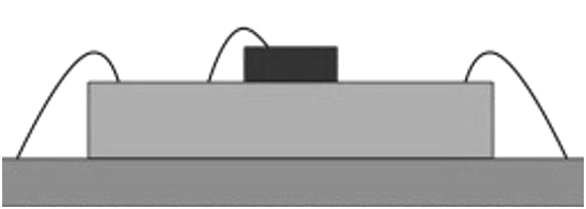
To integrate the clock generator into the microcontroller, Texas Instruments developed a film bulk acoustic wave (BAW) resonator that can be placed on top of the Si chip to form a package system.

This enables researchers and developers in all areas of Texas Instruments to achieve two goals. So far, they have optimized the design of the bulk wave resonator, which produces high quality high frequency oscillations - typically 1200 at 2.5 GHz - and it can be mounted in the housing with the silicon chip.

Volumetric resonators developed by Texas Instruments can be fabricated on silicon substrates using thin film technology. It consists of a piezoelectric layer between two metal electrodes and is surrounded by several layers that act as acoustic reflectors to limit mechanical energy, thereby forming a high quality resonator.

To date, most microprocessors use a clock signal whose frequency is given by an external crystal to produce an accurate clock signal.

Advances in the miniaturization of digital circuits mean that quartz can be considered the largest device in a microcontroller circuit. Until now, it has not been possible to miniaturize an external crystal equivalent to a digital circuit or integrate it with a chip in an IC package.

On the other hand, the RC or LC generator integrated in the microcontroller saves space. They can be integrated directly into the IC, but due to their high tolerance, they are only suitable for a few applications and are hard to be considered as a substitute for quartz.

image.png
Figure 1. A BAW resonator is placed on a Si chip and electrically connected to the semiconductor chip by wire bonding.

Although external MEMS generators are smaller than quartz and avoid their disadvantages, they still require extra space on the PCB. MEMS clocks integrated in the IC housing, such as the BAW resonator developed by Texas Instruments, provide a space-saving alternative.

Texas Instruments chose bulk wave resonator technology because it not only allows accurate clock signal generation, but the materials needed to build BAW resonators are also suitable for semiconductor manufacturing (Table 1).

Technology
Advantages
Disadvantage
Bulk Wave Resonator(BAW)
·    Height Goodness ,   about 1000 at 2.5   GHzallows very small jitter.
·    Height Resonance frequency of 2 GHz to 3   GHz allows it lots clock frequencies bydivision to generate , eg .
 Can out throughthe 2.5   GHz signal of a BAW   resonatorDivision 156.25 MHz, 125 MHz and 100 MHz won be .
·    Very low RMS jitter not from the outsideaffected becomes :   <60 fs (12   kHz - 20 MHz) at 156.25   MHz, <30 fs (12   kHz - 20 MHz) at 1.25   GHz.
·    Integration as   a system in package enablesthe use of standard QFN packages , lowCost and easy to design .
·    Smaller Voting range .
·    Remedy is With oneadditional PLLcircuit 
possible with LC-VCO.
Surface waveresonator (SAW)

·    Exotic Substrate material , not easyto integrate .
·    Lower Frequencies<1 GHz
LC
·    Monolithic integration.
·    Low Costs .
·    Low Quality ,   about 20 at 1   GHz, leadsto high jitter   andphase noise and isstakt depending onexternal Influences .
Table1. Can be used as a comparison of quartz replacement technology (source: Texas Instruments).

Accurate clock signal for reliable communication
Texas Instruments first integrated the BAW resonator into two circuits, a device for synchronizing clock signals in the network (LMK05318) and a microcontroller with a radio transceiver (CC2652RB). Both ICs benefit from the low jitter and low temperature drift and aging of the BAW clock generator.

An internal comparison with the PLL's CC2652RB compensates for temperature drift and aging of the Texas Instruments Volumenwellenresonators, resulting in a deviation of up to ±40ppm from a 48 MHz clock frequency.
For example, Bluetooth, threads and values required in the Zigbee wireless technology specification to achieve reliable data transfer. As another advantage of microcontrollers, Texas Instruments claims that eliminating external quartz can save 12% of printed circuit board area.

However, bulk wave resonators require slightly more energy during operation than clock generators with external quartz. Texas Instruments instructs the microcontroller CC2652RB to have a higher current consumption of 500 microamps from the BAW resonator. Partially compensating them, Texas Instruments is integrated in wireless standards, such as the control of BAW resonators in the protocol stack of the Bluetooth low-power stack.

With the typical intermittent operation of the transmission pause Texas Instruments will have more CC2652RB power requirements with BAW resonance to about 4.4 to the Bluetooth LE connection up to seven percent compared to the CC2652R which requires an external 48-MHz crystal.


What issues need to be considered when designing LED driver circuits?

LED has many advantages such as environmental protection, long life, high photoelectric efficiency, etc. In recent years, the application in...