Thursday, October 31, 2019

What forms of electromagnetic interference

At present, the deteriorating electromagnetic environment has made us pay more attention to the working environment of equipment, and pay more attention to the impact of electromagnetic environment on electronic equipment. From the beginning of design, we integrate electromagnetic compatibility design to make electronic equipment work more reliably.
Electromagnetic compatibility design mainly includes surge (impact) immunity, ringing wave immunity, electrical fast transient pulse group immunity, voltage sag, short-term interruption and voltage variation immunity, power frequency power supply Harmonic immunity, electrostatic immunity, RF electromagnetic field immunity, power frequency magnetic field immunity, pulse magnetic field immunity, conducted disturbance, radiated disturbance, and conducted immunity of RF field induction.
Main form of electromagnetic interference
Electromagnetic interference mainly enters the system through conduction and radiation, affecting system operation. Other methods include common impedance coupling and inductive coupling.
Conduction: Conductive coupling is the coupling of disturbances on one electrical network to another via a conductive medium, which is part of the lower frequency (below 30 MHz). Conductive coupling in our products typically includes power lines, signal lines, interconnects, ground conductors, and the like.
Radiation: The coupling of disturbances on one electrical network to another via a space, which is a higher frequency part (above 30 MHz). The path of radiation is transmitted through space, and the radiation interference introduced and generated in our circuits is mainly the antenna effect formed by various wires.
Common impedance coupling: Mutual interference that occurs when currents of two or more different circuits flow through a common impedance. The disturbance current conducted on the power line and the ground conductor is mostly introduced into the sensitive circuit in this way.
Inductive coupling: Through the principle of mutual inductance, the electrical signal transmitted in one loop is induced to interfere with another loop. Divided into electric induction and magnetic induction.
The corresponding countermeasures should be adopted for the interference caused by these several ways: the transmission adopts filtering (such as the chip head capacitor of each IC in our design is the filtering effect), and the radiation interference adopts the reduction of the antenna effect (such as the signal is close to the ground), Shielding and grounding measures can greatly improve the product's ability to resist electromagnetic interference, and can also effectively reduce electromagnetic interference to the outside world.
Component selection
Our commonly used electronic devices mainly include active devices and passive devices. Active devices mainly refer to ICs and module circuits. Passive devices mainly refer to resistors, capacitors, inductors and other components. The following is a brief introduction to the selection of these two types of components and the issues to be considered in electromagnetic compatibility.
Active device EMC selection
The EMC characteristic of the working voltage is good, the EMC characteristic of the working voltage is good, the delay is large in the range allowed by the design (so-called slow speed), the quiescent current is small, the power consumption is small, and the characteristic is good. The EMC performance of the SMD packaged devices is better than that of the interposer devices.
Passive device selection
Passive devices usually include resistors, capacitors, inductors, etc. in our applications. For the selection of passive components, we must pay attention to the frequency characteristics and distribution parameters of these components.
Passive devices exhibit different characteristics at certain frequencies. Some resistors have inductance characteristics at high frequencies, such as wirewound resistors, low frequency characteristics of electrolytic capacitors, poor high frequency characteristics, and thin film capacitors and ceramic capacitors. High frequency characteristics are good, but usually the capacity is small. Consider the influence of temperature on components, and select devices with various temperature characteristics according to the design principle.
If you want to know more, our website has product specifications for electronic equipment, you can go to ALLICDATA ELECTRONICS LIMITED to get more information
Saturday, October 26, 2019

What is the difference between the LED and OLED screen structure?

The difference between the LED screen and the OLED screen is not only a letter difference, but the imaging technology of the two is completely different.

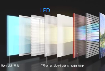
LED screen structure is more complicated
image.png
LED screens and OLED screens have fundamental differences in the principle of illumination.
The full name of the LED is a light-emitting diode. Like the traditional semiconductor industry, LED display screens are a way of controlling the display of semiconductor light-emitting diodes. They are usually composed of a plurality of red light-emitting diodes, which are dominated by the display of lights, thereby realizing text, graphics, images, and animation. Display screen for various information such as video and video signals. Its process cost is high. In addition, LEDs can only be used in the form of point sources.

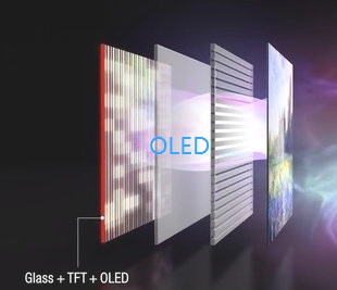
OLED does not require a backlight, and the structure is lighter and thinner.
image.png 
The OLED emits light by driving the organic film itself. OLED is a congenital surface light source technology, and the light emitted can be red, green, blue, white and other monochromatic colors, thereby achieving the effect of full color, belonging to a new principle of illumination. The reason why plasma technology, OLED technology and even the image quality of CRT technology in the early years are praised is mainly because they all have the characteristics of "self-illumination".

Tuesday, October 22, 2019

Connectors in electronics are an essential part

In today's era of so advanced technology, there are many electronic products that we use or touch in real life. Imagine what would happen if there were no connectors in electronic products. The circuits of electronic products should be permanently connected with continuous conductors. Together, for example, an electronic device is to be connected to a power source, and both ends of the connecting wire must be fixedly fastened to the electronic device and the power source by some method (welding).
As mentioned above, both the manufacture of the product and the use of the finished electronic product bring a lot of inconvenience. Taking the LED landscape light as an example, the distance from the power supply to the lamp holder is generally relatively large. If each line is connected from head to tail from the power supply to the lamp holder, it will bring unnecessary trouble to the construction and cause Wire wasted.

Some people may ask questions, directly open a gap from the fire line, connect the conductive parts of the wire together, and then wrap a few layers of insulating glue is not OK? It is not necessary to use a connector. Firstly, most of the insulating tapes are easy to age, and there are safety hazards. Secondly, the mechanical properties of the joints directly connected by wires are very poor. The wires are slightly vibrated and stretched, which is easy to cause an open circuit, and the interface is poorly contacted, which may cause heat generation, which may cause a fire.

Moreover, the outdoor environment is harsh, the requirements of waterproofing, salt-proof and anti-aging will be relatively high, and the insulating rubber will not meet the requirements. But if you use high-performance waterproof connectors in outdoor lighting, it not only simplifies the installation of the power grid, but also all the safety hazards will be reduced to a very low level.

The above example simply illustrates the benefits of the connector, which makes the design and production process more convenient, more flexible, safer, and lowers production and maintenance costs. The emergence of connectors improves the manufacturing process. The connector simplifies the assembly process of electronic products, and simplifies the mass production process. It is easy to repair. If an electronic component fails, the failed component can be quickly replaced when the connector is installed, and the upgrade is easy. Replacing components with connectors, replacing old design flexibility with new, more sophisticated components. Using connectors allows engineers to design and integrate new products, as well as when building components with components, Greater flexibility.

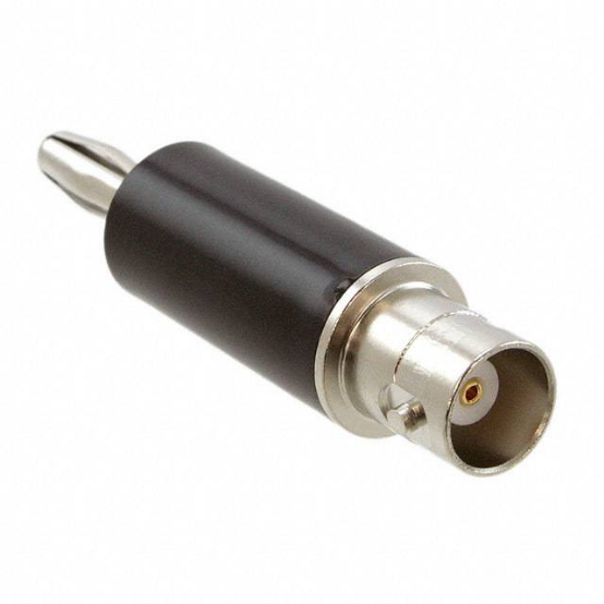
Especially for industrial connectors, sometimes it is more important to be flexible and safe in harsh environments where plugging and unplugging is required. At this time, a simple plug connector with a snap button would be a wise choice.
image.png 

Friday, October 18, 2019

ASICs and FPGAs are not competitors in the field of artificial intelligence chips

In the wave of artificial intelligence chips, in addition to the general-purpose chip CPU and GPU in the traditional sense, special chips such as FPGA and ASIC have become the choice of more and more manufacturers.
In general, such chips are less customizable, and customers cannot choose the chip that suits them according to their own characteristics. However, for the cloud computing, it does not require much customized content while processing the data. This also limits the cloud computing market from a market demand to a relatively fixed market.
Therefore, at this stage of development, the cloud computing market has gradually revealed a monopoly situation. CPUs, GPUs, etc. have divided the market share. It is extremely difficult for other manufacturers to make further advances.
However, different applications and different scenarios have different requirements for chips. How to launch chips in a targeted manner is also being considered by more and more manufacturers.
From the current situation, many people think that there are two solutions in the market, one is a custom solution based on ASIC chips; the other is an FPGA-based programmable solution. Or, for the end-market, FPGA and ASIC are either rivals.
However, the rival of FPGA is not ASIC, because artificial intelligence requires an open chip.
If the CPU and GPU belong to a closed chip, then the unique programmability of the FPGA makes the chip open, while the ASIC is open on the surface, but essentially, after the chip is finalized, It is impossible to change, it is "semi-open".
For the artificial market, the cloud needs to be relatively fixed, and the chip required on the end side needs an open chip according to different landing scenarios. ASIC's "semi-open" indicates that such chips can be developed for specific markets and applications, but because of the increasing cost of chips from design to tape to mass production, it is difficult to have a single market capacity to support ASICs. The chip goes for deeper development.
However, the bitcoin market is a special case. This market is not based on application scenarios. The total market is pure financial games, and there is not much use value. Therefore, it is not difficult to find that when the value of Bitcoin is high, it can support it to develop ASIC chips. When Bitcoin crashes, ASIC chips will be difficult.
This is still the case in the bitcoin market, especially for other smaller markets.
For the artificial intelligence market, the cloud computing needs a closed chip, and the end side needs an open chip. This is the main battlefield of chips such as FPGA. ASIC is only a specific market demand, let alone Be the opponent of FPGA.
But this does not mean that the FPGA can be perfectly applied to the end side, and the FPGA still has a lot of room for improvement.

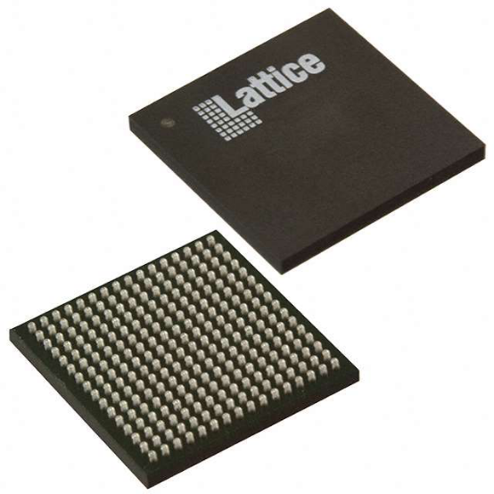
FPGA :LCMXO3L-6900C-6BG256C

image.png

Thursday, October 17, 2019

What is the signal letter displayed on the motherboard?

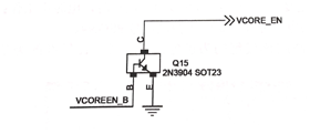
1.Turn on (EN) signal.
Turn on signal is the signal that controls chip to work, abbreviation EN, is abbreviation of ENABLE. Common open signals are high-level on-circuit operation, low-power normally closed circuit (see figure 1). There are also chip-on-off signals called SHDN#, the SHUTDOWN, band # number that indicates low level efficiency, which means that low power is normally turned off, so if you want to turn it on, it must be high.
               image.png
                      Fig.1 EN signal circuit

 The common names of EN signals are EN, ENLL, DVD, VR_Enable, OUTEN, ENABLE, SHDN#, VCORE_EN, VRM_EN, VTT_PWRGD, VRD_EN, etc.
               
2.Power Good (PG) signal.
POWERGOOD, is abbreviated to PG. The good signal of power supply is used to describe the signal of normal power supply, usually when the power level is high, the power supply is normal. For example, the ATX power supply uses gray lines as a good signal for (ATXPWROK) signals, and gray lines are designed to delay hundreds of milliseconds after electrification to indicate that the power supply is normal at a high level. For example, CPU power supply management chip in the normal issue of CPU voltage, will send a good signal to the South Bridge power supply VRMPWRGD chip, indicating that the power management chip work well.
The high level ATXPWROK signal from the ATX power gray line and the VRMPWRGD signal from the power supply chip in the main board will be sent to the Nanqiao chip to indicate that the corresponding power supply is normal, and the Nanqiao chip will issue CPUPWRGD to CPU, after receiving the good power supply signal. A reset signal is then generated to reset the entire motherboard and each device.
The common names for PG signals are PG,PWRGD, PWROK, ATXPWRGD,VTPWRGD,CPUPWRGD, VR_RDY, YRM_PWROK, and so on, as shown in figure 3.
         image.png
                     Fig.2 Powergood
          

3.Clock (CLK) signal.
Clock signal CLK (CLOCK) is the digital circuit working reference, so that each connected equipment to work at a uniform pace. The basic unit of the clock signal is Hz. There is a master clock generation circuit on the motherboard that provides clock signals to all devices on the motherboard. For different devices, the clock circuit sends out different clock signals, such as the frequency of the clock signal given to CPU is above 100MHz. The clock signal frequency for the PCI device is 33 MHz, the clock signal frequency for the PCILE device is 100 MHz, and the clock signal frequency for the USB controller (integrated in the South Bridge chip) is 48MHz. The clock signals of CPU, PCI, PCL-E and so on need the normal power on the motherboard, and the clock chip can be measured by oscilloscope.
The motherboard requires that two connected devices must have the same frequency of clock signals and voltages to communicate, such as memory and North Bridge chips, both of which require the same clock signals and voltages in order to transmit signals normally.

4.Reset (RST) signal.
Reset RST (RESET (abbreviated) is the meaning of a fresh start. Now the device reset signal on the motherboard is from high level to low level jump back to high level. For example, the reset signal of PCI is from 3.3V to 0V and back to 3.3V, which is a normal reset jump process. The reset signal is generally expressed as *** RST#, such as PCIRST#,CPURST#,IDERST#, etc. Reset signal can only be instantaneous low level, the reset signal is high when the motherboard is working normally.
When you say no reset, you usually mean no reset voltage, that is, the reset signal measurement point voltage is 0V.

Monday, October 14, 2019

How to detect whether the trigger circuit related signal is normal?

After the standby condition detection is normal, the trigger signal in the trigger circuit is detected whether the jump-off is normal or not. The common trigger signals are PWRBITN#, SLP_S3#, PSON#. Trigger circuit maintenance methods are as follows.

 (1) First distinguish the main board trigger circuit working mode, common main board trigger circuit work as follows.
Intel, nVIDIA, AMD chipset motherboard: Switch, IO chip, south bridge chip, IO chip green wire.
VIA chipset motherboard: Switch south bridge chip transistor green wire. 
SIS chipset motherboard: Switch South Bridge chip green cable. 
Intel original motherboard: Switch South Bridge chip IO chip, detect CPU green cable.
IBM, DELL motherboard: Switch South Bridge chip IO chip green cable. 

(2) Measuring the corresponding trigger signal. 

a)Most of the motherboards are triggered by IO chips in the existing motherboard maintenance, so to measure the trigger signal you must measure the IO chip-related pins. Common IO chips trigger pin as follows. 
Pin of IT8702, IT8712, IT8716, 1T8718, 1T8720, IT8721, 1T8726, 178728: 67 powered, 75 72 71 76 (GB plus 31). 

IT8758 pin: 2, 31 power, 35 33  32 36. 
Pin position of W83627: 61 Power, 68 67 73 72. 
Pin position of F71872: 67 power, 75 72  71 76. 
Pin position of F71862, 71882, 71883: 68 electricity, 80 81 82 83. 
Pin position of F71889: 65 power supply, 76 77 78 79. 
Note: IT8705, W83697, W83687 are not triggered. 

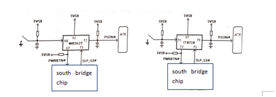
b)The trigger circuit block diagram commonly composed of Huabang and Lianyang I 0 chips is shown in figure 3. 

image.png
(a) Huabang                      (h) Lianyang
figure 3 IO chip trigger block diagram.

Huabang and Lianyang 1O chip corresponding to normal foot jump mode: trigger switch before triggering switch triggering switch after. 
W83627 Series. 
The 68 pin are high level low level high level. 
The 67 pin are high level low level high level. 
The 73-pin is low or high-level continuous high-level. 
The 72-pin is high-level sustained low-level. 
ITE series (except IT8711). 
The 75-pin is high-level low-level high-level. 
The 72-pin is high-level low-level high-level. 
The 71-pin is low or high-level continuous high-level. 
The 76-pin is high-level sustained low-level.

(3) Abnormal maintenance method of trigger signal. 
Using W83627 series IO chip motherboard, trigger circuit maintenance ideas are as follows. a. if the switch does not have a high level, check the pull-up resistance, capacitance, and IO chip of the switch for damage.
b. if the switch has a high level, but presses the switch 68 pin without jumping, check the line (run) from the switch to 68 pin.
c. if the 67 pin in front of the switch do not have 3.3V, check first whether the power supply to the IO chip is normal or not. If normal first change the IO chip, and finally change the South Bridge chip.

Saturday, October 12, 2019

What are the characteristics of LED lights?

image.png
LED lamp beads introduction
LED is called light emitting diode. The terminal voltage of the PN junction constitutes a certain barrier. When the forward bias voltage is applied, the barrier decreases, and the majority carriers in the P and N regions diffuse toward each other. Since the electron mobility is much larger than the hole mobility, a large amount of electrons diffuse into the P region, which constitutes injection of minority carriers in the P region. These electrons recombine with the holes in the valence band, and the energy obtained during the recombination is released in the form of light energy. This is the principle of PN junction illumination.

 LED lamp bead characteristics
1. Voltage: LED lamp bead uses low voltage power supply, the supply voltage is between 2-4V, depending on the product, so it is driven by a higher voltage than the high voltage power supply; it is especially suitable for public places;

2. Current: The working current is between 0 and 15 mA, and the brightness becomes brighter as the current increases.

3. Performance: Energy consumption is reduced by 80% compared to incandescent lamps with the same efficacy.

4. Applicability: Very small, each unit LED small piece is 3-5mm square, so it can be made into various shapes and suitable for variable environment.

6. Response time: The response time of the incandescent lamp is millisecond, and the response time of the LED is nanosecond.

7. Environmental pollution: no harmful metal mercury.

8. Color: Change the current to change color. The LED can easily adjust the energy band structure and band gap of the material by chemical modification method to realize multi-color luminescence of red, yellow, green and blue. For example, a red LED with a small current can turn orange, yellow, and finally green as the current increases.


LED lamp bead application range
LED lamp beads are widely used in lighting production, LED large screen display, traffic lights, decoration, computers, electronic toy gifts, switches, telephones, advertising, urban glory engineering and many other production areas.

If you want to know more, our website has product specifications for LED, you can go to ALLICDATA ELECTRONICS LIMITED to get more information

Friday, October 11, 2019

Electromagnetic interference has those forms

At present, the deteriorating electromagnetic environment has made us pay more attention to the working environment of equipment, and pay more attention to the impact of electromagnetic environment on electronic equipment. From the beginning of design, we integrate electromagnetic compatibility design to make electronic equipment work more reliably.
Electromagnetic compatibility design mainly includes surge (impact) immunity, ringing wave immunity, electrical fast transient pulse group immunity, voltage sag, short-term interruption and voltage variation immunity, power frequency power supply Harmonic immunity, electrostatic immunity, RF electromagnetic field immunity, power frequency magnetic field immunity, pulse magnetic field immunity, conducted disturbance, radiated disturbance, and conducted immunity of RF field induction.
Main form of electromagnetic interference
Electromagnetic interference mainly enters the system through conduction and radiation, affecting system operation. Other methods include common impedance coupling and inductive coupling.
Conduction: Conductive coupling is the coupling of disturbances on one electrical network to another via a conductive medium, which is part of the lower frequency (below 30 MHz). Conductive coupling in our products typically includes power lines, signal lines, interconnects, ground conductors, and the like.
Radiation: The coupling of disturbances on one electrical network to another via a space, which is a higher frequency part (above 30 MHz). The path of radiation is transmitted through space, and the radiation interference introduced and generated in our circuits is mainly the antenna effect formed by various wires.
Common impedance coupling: Mutual interference that occurs when currents of two or more different circuits flow through a common impedance. The disturbance current conducted on the power line and the ground conductor is mostly introduced into the sensitive circuit in this way.
Inductive coupling: Through the principle of mutual inductance, the electrical signal transmitted in one loop is induced to interfere with another loop. Divided into electric induction and magnetic induction.
The corresponding countermeasures should be adopted for the interference caused by these several ways: the transmission adopts filtering (such as the chip head capacitor of each IC in our design is the filtering effect), and the radiation interference adopts the reduction of the antenna effect (such as the signal is close to the ground), Shielding and grounding measures can greatly improve the product's ability to resist electromagnetic interference, and can also effectively reduce electromagnetic interference to the outside world.
Component selection
Our commonly used electronic devices mainly include active devices and passive devices. Active devices mainly refer to ICs and module circuits. Passive devices mainly refer to resistors, capacitors, inductors and other components. The following is a brief introduction to the selection of these two types of components and the issues to be considered in electromagnetic compatibility.
Active device EMC selection
The EMC characteristic of the working voltage is good, the EMC characteristic of the working voltage is good, the delay is large in the range allowed by the design (so-called slow speed), the quiescent current is small, the power consumption is small, and the characteristic is good. The EMC performance of the SMD packaged devices is better than that of the interposer devices.
Passive device selection
Passive devices usually include resistors, capacitors, inductors, etc. in our applications. For the selection of passive components, we must pay attention to the frequency characteristics and distribution parameters of these components.
Passive devices exhibit different characteristics at certain frequencies. Some resistors have inductance characteristics at high frequencies, such as wirewound resistors, low frequency characteristics of electrolytic capacitors, poor high frequency characteristics, and thin film capacitors and ceramic capacitors. High frequency characteristics are good, but usually the capacity is small. Consider the influence of temperature on components, and select devices with various temperature characteristics according to the design principle.
If you want to know more, our website has product specifications for electronic equipment, you can go to ALLICDATA ELECTRONICS LIMITED to get more information
Thursday, October 10, 2019

How do you design a common emitter amplifier circuit?

It is very simple to understand the principle of a common-emitter amplifier circuit. But it is not easy to really design a common-emitter amplifier circuit. Here is a summary of the design steps of the common-emitter amplifier.

1. Design requirements:
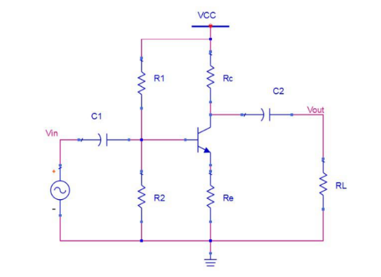
The following figure shows a RC-coupled common-emitter amplifier circuit. For a 1 kHz sinusoidal signal with an input peak-to-peak value of 2V, the load is 100kohm, and a 5x amplification circuit is designed.
image.png
2, design ideas and steps
The first step: First, the power supply voltage VCC must be selected.
In the circuit, the power supply voltage is high, and the power consumption is large. When possible, everyone should continuously reduce the power supply voltage to achieve low power consumption. In an amplifying circuit, the minimum supply voltage depends on the amplitude and amplification of the input signal. For example, to amplify the 2Vpp signal by a factor of 5, the limit VCC also needs to be greater than 10.5V (0.5V for V_ces and V_Re). The larger the supply voltage margin, the smaller the design pressure. Here, the common 15V voltage is taken as VCC.
Step 2: Design the value of Rc
The output impedance Rc of the common-emitter amplifying circuit needs to be set according to the magnitude of the load resistance. The value of the resistor in the circuit must be considered. If the bigger the better, it is better to open the circuit. If the smaller the better, the short circuit is better. The smaller the Rc is, the smaller the output impedance is, and the more stable the amplification factor is after the load is applied. However, the smaller the Rc, the larger the static power consumption of the amplifying circuit, that is, the power consumed without load.

Considering the load condition, set it to one tenth of the load 100kohm, so that 90% of the voltage will be added to the load, which has little effect on the amplification; Rc=10kohm.

The third step: design the value of Re
According to the magnification formula, A=-Rc/Re, the magnification is 5, so, Re=2kohm.

Step 4: Design the input signal bias voltage
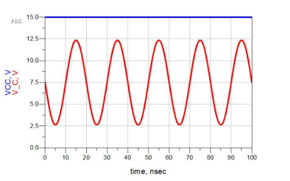
The common-emitter amplifier circuit is reverse-amplified, so the higher the DC offset of the input signal, the lower the output signal; the lower the input signal offset, the higher the output signal is. If there is no special requirement, the output signal can be placed in the center of the power rail (so that the maximum undistorted gain can be obtained), as shown in the figure below.
image.png
According to the DC equivalent circuit and Vc=7.5V, the DC offset Vb of the input signal can be deduced. Here we take the bias voltage Vb = 2.2V.

Step 5: Design the size of R1 and R2
Since the 15V partial voltage gets 2.2V, the higher the resistance power consumption, the lower the input impedance. However, since the voltage divider resistor network also has a branch flowing through the B pole of the triode, R2 must be small enough to ignore the current flowing through the branch. Calculated by beta=100, the equivalent resistance of the branch is 100*. Re=200kohm. Therefore, choose R2=20kohm, which is much smaller than the equivalent resistance of the branch.

According to R2 is 20kohm, R1=116kohm is calculated, 116kohm is not in the E24 series, and the closest R1 is 120kohm. This will bring a little DC error, but because the VCC margin is relatively large, some errors have no effect.

Step 6: Selection of electrolytic capacitors C1 and C2
The electrolytic capacitor must have an impedance to the AC signal close to zero. In other words, the use of electrolytic capacitors is related to the signal frequency. From the filter point of view, the capacitors C1 and R1 || R2 || beta * Re constitute a high-pass filter, as long as the high-pass filter cutoff frequency is lower than 1/10 of the signal frequency, the impedance of the input signal is considered to be 0, here Take C1=120nf. Similarly, the capacitor C2 and the load RL constitute a high-pass filter. As long as the cut-off frequency of the high-pass filter is lower than 1/10 of the signal frequency, the impedance of the output signal can be considered to be 0, where C2=20nf is taken.

If you want to know more, our website has product specifications for the common-emitter amplifier, you can go to ALLICDATA ELECTRONICS LIMITED to get more information
Wednesday, October 9, 2019

IoT Microcontroller for ARM Cortex M33 Bluetooth Multicore MCU

The DA1469x family offers advanced connectivity, allowing developers to prove their equipment and meet the needs of multiple applications in the future.
Dialog Semiconductor has introduced a range of Bluetooth low energy SoCs in the embedded world with the SmartBond DA1469x family. It is a first-line wireless microcontroller based on the ARM Cortex M33.


The new product line DA1469x's Dialog Semiconductor has a core that has been carefully tested according to its capabilities, selecting processes between network devices and communicating three processors.
The DA1469x home-based application processor ARM M33 for power calculation. It provides developers with more powerful application processing capabilities, such as high-end fitness trackers, advanced smart home devices and virtual reality game controllers.
The new dual-range integrated radio transceiver is based on the ARM Cortex-M0+ with a software-programmable packet engine on which the protocol is implemented. With the new Bluetooth 5.1 standard, the transceiver can be precisely positioned with the newly introduced 5.1 angle and exit angle functions. They make it possible to accurately determine the location of the internal equipment, for example to implement functions for building access and remote keyless entry systems.

Processor and sensor controller
The DA1469x improves SoCs, then the M33 application processor and the M0+ Protocol Engine (SNC) are added by the sensor node controller, which is based on the programmable micro DSP. It can autonomously process the data of sensors connected to its digital and analog interfaces independently and wake up the application processor only when needed. In addition to this power-saving feature, the internal power supply provides advanced power management by controlling the various cores and enabling them when needed. The internal power supply has three regulated outputs for the internal block and LDO output to supply external components, so that no separate voltage regulator integrated circuit is required.

The SOC DA1469x family features up to 144 DMIPS (Dhrystone MIPS), 512 kB of RAM, storage protection, floating point units, end-to-end security and a dedicated encryption engine in scalable memory to ensure a variety of advanced smart devices Applications can be implemented through the chipset family. In addition, they are equipped with some key interfaces, including a display driver, audio interface, USB, an accurate ADC, a driver for the vibration motor, two ERM (eccentric rotation mass) and LRA (linear vibration motor), and A programmable stepper motor controller.

The four variants of the new DA1469x product line build the dialogue's success in smart bond products and provide more computing power, resources, range and battery life for a variety of IoT-related consumer applications. Using the series to develop DA1469x work can rely on the dialogue software development kit SmartSnippets, let their tools in hand, they need to develop new SoC applications.

What issues need to be considered when designing LED driver circuits?

LED has many advantages such as environmental protection, long life, high photoelectric efficiency, etc. In recent years, the application in...