The current required for DDR2 and DDR3 memory is large, so most motherboards use switching power step-down mode (PWM).
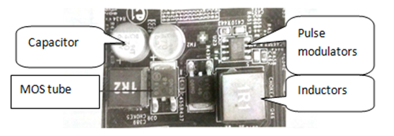
Memory-powered switching power circuits are generally composed of pulse modulators (PWM), MOS transistors, inductors, and electrical memory, as shown in figure 1.

Figure 1 physical diagram of the on-off power supply powered by memory.
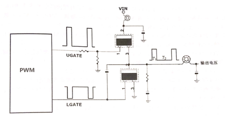
The PWM circuit works as shown in figure 2. The PWM chip adjusts the output voltage by controlling the high-speed on and off of the upper and lower tubes. When the upper tube is turned on, the VIN charges the energy storage circuit of the inductor and capacitor through the upper tube and supplies power to the later stage. When the capacitor and inductor is full of electricity, the PWM chip controls and closes the upper tube, and opens the lower tube so that the energy storage circuit composed of inductor and capacitor can form a closed loop, so that the inductor and capacitor discharge continue to supply power to the later stage (the lower tube constitutes the discharge loop). In fig. 2, T1 is on and T2 is off. It can be seen from the diagram that the output voltage can be effectively controlled by controlling the duty cycle of T1.

Fig.2 The PWM circuit works.


