Friday, August 30, 2019

What is a gas sensor and what is its function and characteristics?

1.The role of the gas sensor.
The device that can sense the change of gas sensing concentration is called gas sensor. Gas sensors are widely used in petroleum, mining, machinery, chemical and other light and heavy industries as well as ordinary families about gas poisoning and fire, detection, alarm and control of accidents such as explosion and air pollution. In industrial production and people's daily life, gas sensors are widely used to detect the leakage of combustible gases and toxic gases, in case of air pollution, explosion, fire, poisoning, etc.  There are many kinds of gas sensors , and the most common ones are semiconductor gas sensors.

2.The characteristics of the gas sensor.
Semiconductor gas sensor is the core of semiconductor gas sensor. It is made of the characteristic that the semiconductor material SnO 2 can adsorb the gas to change its resistance. When the detected gas is adsorbed on its surface, the proportion of conductive electrons in the contact interface of the semiconductor crystallite particles will change, so that the resistance value of the gas sensor will be changed measuring the concentration of the gas changes, so the gas concentration can be converted into the change of the Telecom number. This reaction is reversible and therefore reusable.
In order to speed up the reaction and achieve high sensitivity, it is usually necessary to heat the gas sensor with electric current through the heating wire. The heating temperature varies with the material used by the gas sensor. When the gas sensor starts heating in the clean air, the resistance drops sharply, and the stable value is reached after a few minutes, which is called the passive period stabilization time. When the resistance of the gas sensor is in the stable value, it will change with the adsorption of the detected gas. The variation of resistance depends on the type of semiconductor. The resistance of P-type semiconductor gas sensor increased, and the resistance of N-type semiconductor gas sensor decreased. After the gas sensor is heated, the resistance in the normal air is the static resistance Ro, and the resistance value of the gas sensor is Rx, the ratio of Ro to Rx is called the sensitivity of the gas sensor. When the gas sensor is in contact with the detected gas, the time of its resistance changing from Ro to Rx is called the response time; when the gas is removed, the time of recovery from Rx to Ro is called recovery time.

3.Choose a gas sensor in use.
(1)The sensitivity of the measured gas is high, and the variation of resistance per unit gas concentration is large.
(2) Good selectivity for single or multiple measured gases is less dependent on the temperature of the environment.
(4) Good moisture resistance.
(5) Long life.
To understand their aging mechanisms, they can predict their lifespan.

4.Detect the gas sensor.
 Add voltage to the gas sensor, when the gas sensor is connected to the circuit, the voltmeter pointer should be deflected in the negative direction and go back to zero after a few seconds, and then gradually rise to a stable value, indicating that the gas sensor has reached the preheating time. The ammeter should be indicated within 150mA, with some gas (such as alcohol, liquefied gas and so on) aiming at the gas sensitivity. Probe, use a multimeter to measure the voltage at both ends of Uo.
The gas should change, no change is bad. (the greater the amplitude of the voltmeter is, the better the performance of the gas sensor.)

If you want to know more, our website has product specifications for gas sensors, you can go to  ALLICDATA ELECTRONICS  LIMITED to get more information

Gas Sensors CCS811B-JOPD500
 LOW POWER DIGITAL SENSOR FOR INDAir Quality Sensor I²C

CCS811B-JOPD500 Allicdata Electronics

Thursday, August 29, 2019

New superconducting materials needed to develop future computers have been discovered.

Researchers at the Karlsruhe Institute of Technology (KIT) hope to further develop future computers. This requires superconducting materials. This material has now been discovered.

Classic computers only perform one calculation step after another. Quantum computers, on the other hand, work very fast and can perform multiple computational steps simultaneously. Information carriers are so-called "qubits". They not only have the binary values "1" and "0" of the classic computer architecture, but also have values between them. This is achieved by a quantum mechanical superposition of states called superposition principles. However, it is difficult to maintain this state. Now, KIT researchers have used a quantum circuit material that retains this value longer than previously used materials: granular aluminum, or grAl for short.

Granular aluminum as a superconductor
Granular aluminum is a superconductor. These materials have no electrical resistance at very low temperatures and therefore can conduct electricity without loss. With new materials, scientists are committed to quantum computing. This is a major challenge so far. Superconducting materials are critical to maintaining the quantum state of the drill bit and joining them together. Companies such as IBM, Intel or Microsoft are already working to expand the scale of superconducting quantum processors.

High coherence time
The difficulty in maintaining the quantum state lies in the interaction with the environment, which may lead to the decline of the coherent state. The more qubits you use, the more difficult it is to maintain consistency. Granular aluminum acts as a superconductor and is known by researchers as Fluxonium qubits with a coherence time of 30 μs. During this time, more than one thousand logical operations can be performed. The researchers explained that this may increase the performance limits of previous quantum computers.

This article is from Allicdata Electronics Limited.

Wednesday, August 28, 2019

Comparison of advantages of OLED and QLED

The Samsung VD business unit is developing a next-generation TV roadmap that plans to skip OLEDs directly into QLEDs. “Recently, such news from the Korean media has stirred up waves and discussions in the display industry.

For Samsung's strategy, many people question QLED, which is the existing quantum dot TV on the market. It is only a technical upgrade in the LCD field, and cannot be compared with OLED. There is also a voice questioning the reason why Samsung chose QLED, which is an expedient measure after the big-screen OLED technology is unable to catch up with LG. The technical confrontation is used to disperse the market attention of OLED, and the promotion of technological progress is limited.
Such an interpretation may be one-sided. In fact, QLED, which is Samsung's next-generation display technology, is a new display technology that combines the advantages of traditional LCD and OLED.
 image.png

As we all know, the quantum dot used by QLED is a kind of semiconductor nanocrystal. When stimulated by light or electricity, the quantum dot emits colored light. The color of the light is determined by the composition and size of the quantum dot, so it can be changed. The quantum dot morphology yields a high-peak, solid-color light that includes red to blue light, and has a congenital absolute advantage in color. The two application directions of quantum dots in the field of display technology are often confused.
The first is Quantum Dots-Backlight Unit (QD-BLU) based on quantum dot photoluminescence, which is the solution adopted by quantum dot TV on the market. The purpose is to solve the problem that the backlight of ordinary LCD TV is not enough. The problem of brightening, this color deviation is reflected in the screen image, the user will feel that the surface is cold or warm, and the best visual experience is not achieved. Using blue LEDs to obtain high-purity white light through optical materials (QDEF diaphragms) with red and green quantum dots, this problem is well solved, and at the same time, very beautiful colors are restored, which belongs to the field of quantum dots technology applied in the field of LCD. A compromise solution.

Samsung's current QLED research and development refers to the second type of quantum dot application: Quantum Dots Light Emitting Diode Display (QLED) based on electroluminescence characteristics, which belongs to quantum dot display technology. More advanced applications in the field. It is no longer that blue light produces a white light to illuminate the liquid crystal screen through a layer of quantum dot material, but is electrically driven to make the quantum dot itself emit light and produce images by color mixing, eliminating the need for liquid crystal, color film, and eliminating the backlight unit. This makes QLED and OLED have similar principles in display mode.

At the same time, QLED has several advantages over OLED:
1. Because the process is complicated, the production yield is too low has been a problem that large-screen OLED is difficult to overcome, and the QLED process is relatively simple, and has innate advantages in mass production.
2. QLED color performance is more perfect, color gamut can easily reach the most stringent color standard BT202090% or more, while OLED TV color gamut is far more than traditional LCD TV, but under the BT2020 standard, about 70%.
3. Since OLEDs use organic materials, the different lifetimes of the three luminescent materials are their insurmountable fatal injuries. The quantum dot crystal is non-organic, so the working state is more stable, the life is longer, and the cost is lower.
4. Under the same quality, the energy saving of QLED is expected to reach 2 times that of OLED screen.
Cost, production, color, energy consumption, the four major differences between QLED and OLED. In comparison, QLED is not just more "one point" than OLED. Compared with LG's struggling on the big-screen OLED, the situation is not good, Samsung seems to be a bold decision on QLED, think about it, maybe it is a good step in the chest.
Of course, QLED is still in the stage of technology research and development, and it must have some difficult problems to overcome, and it is expected that products will be available only three years later. During this period, whether OLED technology will have a leap-forward development to overcome its own shortcomings, whether QLED technology will encounter bottlenecks in development, it is hard to predict. However, as consumers return to the essence of television and pursue the quality of the face, the next generation of display technology may not be so important. It is the core of competition to provide the best display in a cost-effective form. QLED and OLED are two of the most advantageous technical disputes, leaving us with a lot of imagination space about the future display form. This is the most exciting part.

Monday, August 26, 2019

How to distinguish the positive and negative poles of the primary battery?

Primary battery working principle
The primary battery reaction is an exothermic reaction, generally a redox reaction, but unlike the general redox reaction, electron transfer is not accomplished by an effective collision between the oxidant and the reducing agent, but the reducing agent is lost on the negative electrode. The electron undergoes an oxidation reaction, and electrons are transported to the positive electrode through an external circuit, and the oxidant undergoes an electron reduction reaction on the positive electrode to complete electron transfer between the reducing agent and the oxidant. The directional movement of ions in the solution between the two poles and the directional movement of electrons in the external conductor constitute a closed loop, so that the two electrodes react continuously, an ordered electron transfer process occurs, and a current is generated to convert the chemical energy into electrical energy.

However, it should be noted that the non-redox reaction can be designed as a primary battery. From the perspective of energy conversion, the primary battery is a device that converts chemical energy into electrical energy. From the perspective of chemical reaction, the principle of the primary battery is that the electrons lost by the reducing agent in the redox reaction are transferred to the oxidant via the external wire to make the redox reaction. Performed on two electrodes separately.

The conditions that make up the primary battery
(1) the electrode materials are all inserted into the electrolyte solution;
(2) The two poles are connected to form a closed circuit;
(3) There are two kinds of metals (or one type of non-metal element or metal oxide) which are different in activity;
(4) Internal conditions: The redox reaction can be spontaneously carried out.
image.png
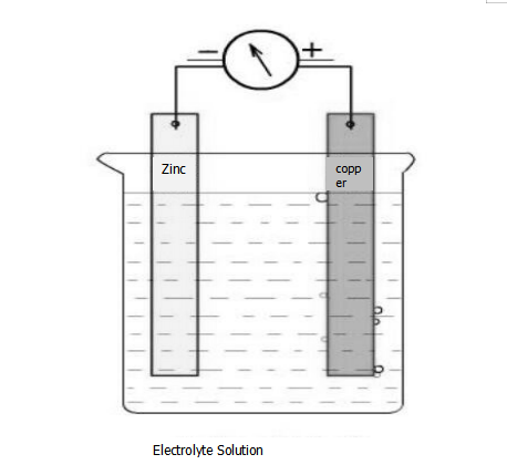
As shown above, the primary battery consists of:
(1) When the electrolyte solution is a CuSO4 solution: the Zn electrode is a negative electrode, the electrode reaction is Zn-2e- = Zn2+, the reaction is an oxidation reaction; the Cu electrode is a positive electrode, and the electrode reaction is Cu2+ + 2e- = Cu, The reaction is a reduction reaction.
(2) When the electrolyte solution is dilute H2SO4: the Zn electrode is a negative electrode, the electrode reaction is Zn-2e- = Zn2+, the reaction is an oxidation reaction; the Cu electrode is a positive electrode, and the electrode reaction is 2H+ + 2e- = H2 , This reaction is a reduction reaction.

Judging the positive and negative of the primary battery
1. Judging by whether or not the electrode material is dissolved. The negative electrode of the primary battery may be dissolved, and the positive electrode must not be dissolved; on the contrary, the electrode that gains weight or has bubbles is positive.

Hitachi integrates AI in automotive stereo cameras to enhance night pedestrian detection

Hitachi Automotive Systems said it has applied artificial intelligence (AI) technology to stereo cameras, which are designed for automotive automatic braking. The camera uses hundreds of thousands of data as "teacher data" to achieve night pedestrian detection. At present, various competitors are developing sensors that support AI. Hitachi Automotive Systems will supply this new sensor to Suzuki Motor Co., Ltd. in order to lead the commercialization of AI sensors.

According to the company, the new sensor's performance is much better than its competitors' products, able to detect pedestrians at night, and then the car can automatically brake, more braking performance than vehicles equipped with Israel Mobileye's main image processing chip EyeQ3 it is good.

Previously, Hitachi’s cameras were “rule-based” to identify objects, ie developers needed to set conditions manually, as did other companies’ products. However, the "rule-based" approach complicates conditions and makes it difficult to support nighttime object detection. This time, Hitachi uses machine learning technology to effectively find conditions in large amounts of data.

In general, a stereo camera uses two left and right cameras to take two images, and then uses the parallax between the two images to detect the shape of the object and the object located in front of the vehicle, and then use pattern recognition to determine the detected object. Whether it is a pedestrian. The stereo camera of Hitachi Automotive Systems will use machine learning to perform image recognition.

Hundreds of thousands of "teacher data" are stored in the image processing microcomputer of the new camera, and then the image taken by the camera is compared with "teacher data" to determine whether the object is a pedestrian. Previously, the stereo camera of Hitachi Automotive Systems used the normal pattern recognition method, which uses multiple images for judgment.

Even if the pedestrian is only illuminated by the headlights of the car or the entire body of the pedestrian can be seen, and the brightness of each body part is different, the camera uses machine learning, which is easier to detect than the traditional pattern recognition method.

The Hitachi Automotive System also increases the dynamic detection range of the CMOS sensor, reducing the F value of the lens (the smaller the F value, the larger the aperture) and doubling the sensitivity of the camera. Thanks to its dynamic range of motion detection, the camera captures both bright and dark objects. And because the F value is smaller, the camera is more likely to find pedestrians in the dark.

When machine learning techniques are applied to image recognition processing, the amount of data that needs to be processed is increased. In order to solve this problem, the Hitachi Automotive System has modified the microcomputer of the stereo camera to improve its performance. The previous stereo camera used three microcomputers for image processing, image recognition, and vehicle control. The new stereo camera of Hitachi Automotive Systems integrates only two microcomputers for image processing and image recognition. Then, the microcomputer for image recognition is upgraded from a single core to a dual core. As the number of cores increases, the microcomputer can not only use machine learning technology, but also improve the processing speed of image recognition.

Monday, August 19, 2019

GND( ground) resistor value measured by a multimeter

In ATX power maintenance, it is often necessary to use a multimeter; to measure the ground resistor of the test points.            
For ac high voltage input side: select the diode block of the multimeter; connect the red pen to the negative pole of the whole bridge, and test the test points of the black pen. At this point, the multimeter; will have a reading known in this article as the "ground resistor value on the high voltage side of the ATX power supply. For the dc low voltage output side: select the multimeter; diode block, red pen connection output terminal ground, black pen contact point. At this point, the multimeter; will also have a reading, which in this book is referred to as the "ground resistor value on the low voltage side of the ATX power supply.

In a word, according to the selected reference point, the ground resistor value of ATX power supply is defined as "ground resistor value of high voltage side and ground resistor value of low voltage side".      
     
Since the ground resistor value can be used as the basis for maintenance, it means that the ground resistor value must reflect a certain essential concurrent of the test point in the circuit, and the 'of whether this essential property is normal or not can effectively clarify the point of failure.       
    
Not. Strictly speaking, the earth resistor value is essentially the equivalent internal resistor of the circuit network between the "negative pole" or "ground" and the "test points" of the circuit board.            

Real circuits are network like, and there are many nodes on the network. According to the venin’s theorem in electricity, a two - terminal network in each network can be equivalent to a resistor (internal resistor), regardless of its internal structure. The two ends of the equivalent resistor are the two ends of the sub network. When a multimeter; is used to measure the earth resistor of the two-terminal network, the value represents the "equivalent resistor".            
         
First, whether or not there is a resistor value to the ground reflects whether the line has been connected normally. In general, the current must be able to flow back to the main board from the test scores, otherwise there will be a break. Therefore, if a test point does not have a ground resistor value, it is not connected to the ground or the negative pole, and for a circuit board that does not drop off, there are indeed but few such signals.             Second, for specific test points, the earth resistor value cannot be too small or even small to the ground or to the negative short circuit, nor can it be too large or even too large to open the road. It will have a normal value, which is determined by the circuit in which the test point is located. If the earth resistor value of a test point is obviously deviated from the normal value, the fault element can be clearly determined in the circuit in which the test point is located, which is the theoretical basis for judging the possible existence of the fault element by using the ground resistor value.            
The above two points are the basic value of the ground resistor value in maintenance.             The bags in voltage caused by the resistor between the pension and the contact resistor between the pension and the measuring points can sometimes not be ignored when the earth resistor value is actually measured. For errors caused by resistor between pen, in the case of a digital multimeter; the relative measurement function provided by the multimeter; itself can be used to zero. For the contact resistor between the meter pen and the measuring points, the tip of the meter pen should be used to contact the measuring points reliably as far as possible.

This article is from Allicdata Electronics Limited.

Wednesday, August 14, 2019

Do you know how to choose electrolytic capacitors?

Electrolytic capacitors are one of the most important devices in primary and secondary loop filter circuits in switching power supplies. Generally, the equivalent circuit of an electrolytic capacitor can be considered as a series connection of an ideal capacitor with a parasitic inductance and an equivalent series resistance, as shown in FIG.
image.png
Figure 1 equivalent circuit of electrolytic capacitor
As is known, switching power supplies are the main power source for today's information appliances, making a great contribution to the small size and lightness of electronic devices. Switching power supplies continue to be smaller, lighter, and more efficient, and are increasingly used in electronic devices, and the penetration rate is increasing.
Capacity and volume

Since electrolytic capacitors are mostly wound structures, it is easy to expand the volume, so the capacitance per unit volume is very large, several times to several tens of times larger than other capacitors. However, the acquisition of large capacitance is at the expense of volume expansion. Modern switching power supplies require more and more efficient and smaller and smaller volumes. Therefore, it is necessary to find new solutions to obtain large capacitance and small size volume of capacitors.

Once an active filter circuit is used on the primary side of the switching power supply, the environment in which the aluminum electrolytic capacitor is used becomes more severe than before:

(1) The main switch of the inverter generates heat, which causes the ambient temperature of the aluminum electrolytic capacitor to rise;

(2) The high-frequency pulse current is mainly a pulsating current of 20 kHz to 100 kHz, and is greatly increased;

(3) The converter uses a booster circuit, so it is required to withstand high voltage aluminum electrolytic capacitors. As a result, the aluminum electrolytic capacitor manufactured by the prior art has to select a larger-sized capacitor because it absorbs a larger pulsating current than ever before. As a result, the power supply is bulky and difficult to use for miniaturized electronic equipment.

In order to solve these problems, it is necessary to research and develop a new type of electrolytic capacitor, which is small in size, high in voltage resistance, and allows a large amount of high-frequency pulse current to flow. In addition, this electrolyticcapacitor operates in a high temperature environment and has a long working life.

Withstand temperature and life

In the switching power supply design process, it is inevitable to choose the applicable capacitor. For medium and large-capacity products of 100 μF or more, aluminum electrolytic capacitors are the most widely used because they are inexpensive. However, significant changes have occurred in recent years, and situation of avoiding using of aluminum electrolytic capacitors is increasing.

 One reason for this change is that the life of aluminum electrolytic capacitors tends to be a weak link in the entire device. The engineer of the power module manufacturer said: "For aluminum electrolytic capacitors, such a component with limited life, if it is not necessary, try not to use it." Because the electrolyte inside the aluminum electrolytic capacitor will evaporate or cause chemical changes, resulting in a decrease in electrostatic capacity or The equivalent series resistance (ESR) increases, and the performance of the capacitor will definitely deteriorate over time.

The life of an electrolytic capacitor is directly related to the ambient temperature at which the capacitor is operated for a long period of time. The higher the temperature, the shorter the life of the capacitor. Ordinary electrolytic capacitors have been damaged at an ambient temperature of 90 °C. However, there are many types of electrolytic capacitors that have a high operating temperature. When the ambient temperature is 90 ° C, the ratio of the alternating current to the rated pulse current through the electrolytic capacitor is 0.5, the lifetime is still 10000 h, but if the temperature rises to At 95 ° C, the electrolytic capacitor is damaged.

Therefore, when selecting a capacitor, it should be selected according to the specific ambient temperature and other parameter indicators. If the influence of the ambient temperature on the life of the capacitor is neglected, the reliability and stability of the power supply operation will be greatly reduced, and even the equipment will be 

Friday, August 9, 2019

Is Facebook's cloud storage a welfare or a trap?

Facebook, which has been dissipated by people all over the world for a long time, has tried its best to save its reputation in the near future. In addition to constant apologies and various privacy commitments, Facebook has also played a variety of tricks on the features of its products. For example, Facebook has been on the dating function a few days ago, trying to become into the "Matchmaker" to lead the red line.

And right now, Facebook has introduced new features including story files and cloud storage. The benefits of these new features are certainly many, but given Facebook’s previous mistakes, it’s hard to let users trust it 100%.

 image.png
Facebook is mainly doing several updates on the app, which will help users better "create and save memories." These updates allow users to save photos and videos directly to an account in the Facebook cloud, send voice messages to friends, and archive their favorite Facebook stories. Specifically, these updates are mainly for users to "save first and then do" - to be able to share photos, stories, etc. directly in Facebook, and then process them after time.

Among them, Facebook camera will enable two of the three new features. After taking a photo or video with a Facebook camera, the user can see a new option to save the photo or video directly to a Facebook account. Photos and videos saved to your Facebook account can only be seen when the user logs in to Facebook - this is called privacy protection.

Another feature allows users to archive their stories, like Facebook cameras, which can be kept secret. Facebook believes that the ability to upload to cloud storage space may convince regions outside of North America, Europe, and Asia to use story features more frequently.

In this regard, Facebook related product director Connor Hayes said, "Save photos and videos can be used to save content that you want to post later. Therefore, users do not have to edit or post photos and videos when they are out with friends, but can Share it in your free time.” But it also means that the new gameplay launched by Facebook is actually controlling user sharing. Photos, videos, stories, etc. uploaded in the Facebook cloud storage space will be "controlled" by Facebook before being released.
 image.png
It is undeniable that some of the features that Facebook launched this time are more like "welfare" and may be welcomed by some users. Especially for users who use entry-level devices, they often live in low-bandwidth Internet areas or have limited mobile space. Facebook's new features help save local storage on storage-limited entry-level devices. After all, these users must delete a photo before they can share a new photo.

Perhaps this is why the media broke the news that Facebook's new features will first be launched to Indian users - after all, the Internet infrastructure there is generally, and the smartphones in the hands of users are mostly low-end models. According to the media, these features will be introduced to other countries and regions in the future.

These new features will undoubtedly have many benefits for Facebook, such as it is possible to get more audio files, photos and videos in order to get more profit. Can't blame the industry for having such "malicious speculation", just because Facebook 

Thursday, August 8, 2019

Comparison of OLED and QLED and comparison of advantages

The Samsung VD business unit is developing a next-generation TV roadmap that plans to skip OLEDs directly into QLEDs. “Recently, such news from the Korean media has stirred up waves and discussions in the display industry.

For Samsung's strategy, many people question QLED, which is the existing quantum dot TV on the market. It is only a technical upgrade in the LCD field, and cannot be compared with OLED. There is also a voice questioning the reason why Samsung chose QLED, which is an expedient measure after the big-screen OLED technology is unable to catch up with LG. The technical confrontation is used to disperse the market attention of OLED, and the promotion of technological progress is limited.
Such an interpretation may be one-sided. In fact, QLED, which is Samsung's next-generation display technology, is a new display technology that combines the advantages of traditional LCD and OLED.
 image.png

As we all know, the quantum dot used by QLED is a kind of semiconductor nanocrystal. When stimulated by light or electricity, the quantum dot emits colored light. The color of the light is determined by the composition and size of the quantum dot, so it can be changed. The quantum dot morphology yields a high-peak, solid-color light that includes red to blue light, and has a congenital absolute advantage in color. The two application directions of quantum dots in the field of display technology are often confused.
The first is Quantum Dots-Backlight Unit (QD-BLU) based on quantum dot photoluminescence, which is the solution adopted by quantum dot TV on the market. The purpose is to solve the problem that the backlight of ordinary LCD TV is not enough. The problem of brightening, this color deviation is reflected in the screen image, the user will feel that the surface is cold or warm, and the best visual experience is not achieved. Using blue LEDs to obtain high-purity white light through optical materials (QDEF diaphragms) with red and green quantum dots, this problem is well solved, and at the same time, very beautiful colors are restored, which belongs to the field of quantum dots technology applied in the field of LCD. A compromise solution.

Samsung's current QLED research and development refers to the second type of quantum dot application: Quantum Dots Light Emitting Diode Display (QLED) based on electroluminescence characteristics, which belongs to quantum dot display technology. More advanced applications in the field. It is no longer that blue light produces a white light to illuminate the liquid crystal screen through a layer of quantum dot material, but is electrically driven to make the quantum dot itself emit light and produce images by color mixing, eliminating the need for liquid crystal, color film, and eliminating the backlight unit. This makes QLED and OLED have similar principles in display mode.

At the same time, QLED has several advantages over OLED:
1. Because the process is complicated, the production yield is too low has been a problem that large-screen OLED is difficult to overcome, and the QLED process is relatively simple, and has innate advantages in mass production.
2. QLED color performance is more perfect, color gamut can easily reach the most stringent color standard BT202090% or more, while OLED TV color gamut is far more than traditional LCD TV, but under the BT2020 standard, about 70%.
3. Since OLEDs use organic materials, the different lifetimes of the three luminescent materials are their insurmountable fatal injuries. The quantum dot crystal is non-organic, so the working state is more stable, the life is longer, and the cost is lower.
4. Under the same quality, the energy saving of QLED is expected to reach 2 times that of OLED screen.
Cost, production, color, energy consumption, the four major differences between QLED and OLED. In comparison, QLED is not just more "one point" than OLED. Compared with LG's struggling on the big-screen OLED, the situation is not good, Samsung seems to be a bold decision on QLED, think about it, maybe it is a good step in the chest.
Of course, QLED is still in the stage of technology research and development, and it must have some difficult problems to overcome, and it is expected that products will be available only three years later. During this period, whether OLED technology will have a leap-forward development to overcome its own shortcomings, whether QLED technology will encounter bottlenecks in development, it is hard to predict. However, as consumers return to the essence of television and pursue the quality of the face, the next generation of display technology may not be so important. It is the core of competition to provide the best display in a cost-effective form. QLED and OLED are two of the most advantageous technical disputes, leaving us with a lot of imagination space about the future display form. This is the most exciting part.

Tuesday, August 6, 2019

New amplifiers with audio applications - IC and multi-chip modules

Infineon is combining its existing line of amplifiers with audio applications - IC and multi-chip modules. Four new Merus brand IC amplifiers have been proposed.

With its new "Merus" brand for audio amplifier ICs, Infineon wants to highlight the advantages of its amplifier ICs:
1. When the sound is generated in the speaker, the heat is not distributed;
2. Can't see, but can hear it;
3. Small and light;
4. Be flexible and configurable, but not just delicate and difficult to use.

The Merus amplifier is based on a new technology: multi-stage switching technology for Class D audio amplifiers, comparable to multi-level converter technology. Not only does it provide high efficiency, but it also has a positive impact on other audio amplifiers such as sound quality, size, output power, electromagnetic emissions and component costs.

Under the new Merus brand, Infineon bundles its amplifier ICs for audio applications.
Infineon is modulating the new Class D audio amplifier to control the power level of the analog five-speed converter. These multistage Class D amplifiers use additional power MOSFETs (integrated in the IC) and capacitors compared to conventional amplifiers.
This technique makes it possible to output an audio signal with a higher granularity, ie with a higher switching frequency and a scalable output signal level. Another advantage of multi-stage Class D amplifiers: they allow for smaller designs and sleep modes with virtually no measurable switching losses.

Four new Merus amplifiers
Based on the new modulation technology, Infineon introduces one of four integrated multi-stage class D audio amplifiers: the MA12040 and MA12070 with analog audio inputs, MA12040P and MA12070P with digital inputs (I 2 S). They are satisfied with power consumption in the 250 mW range and have no output filter. Therefore, they are particularly suitable for portable battery powered devices and for applications with limited installation space - if there is no space for the heat sink and the output filter is present.

The new Merus Class D amplifiers from the Infineon MA12040 / P and MA12070 / P support up to four channels.
Traditional Class D amplifiers operate only at higher volume levels and are more efficient. A realistic and typical audio playback that requires an average of about 1 watt of output power for itself is much more power than the IC of the first generation Merus multi-stage class d audio amplifier now presented.
The new audio amplifier IC supports up to four channels in the mode PBTL (parallel bridge load), BTL (bridged load) or SE (single-ended) can be configured. In PBTL mode, a single monolithic IC can deliver up to 160 W of peak power - maximum. 16 A load current. Alternatively, a four-channel IC can also be used in a 2.1 system, for example, two to drive a 20 watt range speaker (SE mode) and a 40 W woofer (BTL mode).
The new Merus Class D amplifiers, the MA12040/P and MA12070/P, have an integrated digital power supply with low distortion (THD + N = 0.003%) and low EMI emissions. They are protected by a variety of built-in functions: undervoltage shutdown (UVLO), short/overcurrent and DC protection, and warning and error messages when overheating. Infineon offers an integrated Merus Class D audio amplifier IC in a thermally optimized 64-pin QFN package with EPAD (exposed thermal pad).


The role of the transformer in the ATX power supply

The voltage transformer plays a role from front to back in the ATX power supply. The electrical energy input from the primary winding is converted into magnetic energy stored in the core. The magnetic field stored in the transformer core requires a secondary winding output to the rear stage at a "suitable" time via a voltage-varying secondary winding. So, what's the right time? Let's analyze this problem through real-life examples.

1.Cases of  reservoir storage for power generation.
 After a certain amount of water is stored in the reservoir, it can start to generate electricity. At the same time, upstream incoming water can continue to flow into the reservoir and accumulate. This means that there are inputs (upstream water) at the same time as output (power generation) for reservoirs linking up and down.

2.Cases of charging and discharging of rechargeable battery

 After the rechargeable battery has run out of power, it needs to be recharged. Only after recharging, can it be installed into the device to provide the equipment with normal electrical energy.
This means that there is no output (discharge) for a rechargeable battery with input (charge) at the same time.
But why many battery-powered devices (such as laptops) can be charged at the same time?This is actually an illusion, because it is the AC 220V, not the rechargeable battery, that supplies the device with normal power at the moment.

So, is the switching transformer, like reservoir storage, able to output electricity through secondary windings at the same time as charging, or is it possible to output electrical energy through secondary windings after charging and discharging of rechargeable batteries? The answer is: yes, just avoid oversaturation of the core of the switching transformer It is referred to as "forward" (analogy to reservoir energy reserve) in the process of transformer energy conversion which outputs electrical energy through secondary windings at the same time as the primary winding is charged with energy. This is referred to as "fly back" (analogy to charging and discharging of a rechargeable battery) for a transformer that converts energy after the primary winding is charged and then outputs electricity through the secondary winding.

Visible, "forward" and "fly back" are not in fact based on the direction of energy transfer (the direction of any switching power supply is fixed, from the primary winding to the secondary winding), It's a distinction based on the transmission time of energy. Therefore, forward and fly back are essentially the concepts of time related to energy storage, transfer (release).
For "single-transistor forward" and "double-transistor forward" ATX power supplies, the primary switching transformer, while charging the primary windings, has begun to output electricity to subsequent rectified circuits through secondary windings. This is the meaning of "forward" in "single-tube forward" and "double-tube forward".

"fly back" is suitable for low power applications, while "forward" is more suitable for higher power applications. In the ATX power supply, the auxiliary power supply is small, basically uses the "fly back", and the main power supply is large, basically uses "forward". Although there is no word "forward" in the "two-tube and half-bridge" topology, it is actually a form of "forward".

This article is from Allicdata Electronics Limited. Reprinted need to indicate the source.

What issues need to be considered when designing LED driver circuits?

LED has many advantages such as environmental protection, long life, high photoelectric efficiency, etc. In recent years, the application in...